LMX25120967EVAL/NOPB National Semiconductor, LMX25120967EVAL/NOPB Datasheet - Page 7
LMX25120967EVAL/NOPB
Manufacturer Part Number
LMX25120967EVAL/NOPB
Description
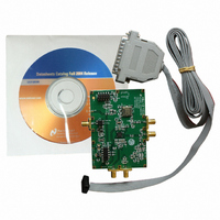
EVALUATION BOARD FOR LMX25120967
Manufacturer
National Semiconductor
Series
PLLatinum™r
Datasheets
1.LMX2512LQ0967NOPB.pdf
(18 pages)
2.LMX2430EVAL.pdf
(8 pages)
3.LMX25120967EVALNOPB.pdf
(24 pages)
Specifications of LMX25120967EVAL/NOPB
Main Purpose
Timing, Frequency Synthesizer
Embedded
No
Utilized Ic / Part
LMX2512
Primary Attributes
Single Fractional-N and Integer-N PLL with VCO
Secondary Attributes
967MHz, CodeLoader Graphical User Interface
Lead Free Status / RoHS Status
Lead free / RoHS Compliant
Other names
*LMX25120967EVAL
*LMX25120967EVAL/NOPB
LMX25120967EVAL
*LMX25120967EVAL/NOPB
LMX25120967EVAL


Functional Description
GENERAL DESCRIPTION
LMX2502/12 is a highly integrated frequency synthesizer
system that generates LO signals for PCS and Cellular
CDMA applications. These devices include all the functional
blocks of a PLL, RF VCO, prescaler, RF phase detector, and
loop filter. The need for external components is limited to a
few passive elements for matching the output impedance
and bypass elements for power line stabilization.
In addition to the RF circuitry, the IC also includes IF fre-
quency dividers, and an IF phase detector to complete the IF
synthesis with the external VCO and the loop filter. Table 1
summarizes the counter values used to generate the default
IF frequencies.
Using a low spurious fractional-N synthesizer based on a
delta sigma modulator, the circuit can support 10 kHz chan-
nel spacing for PCS and Cellular CDMA systems.
The fractional-N synthesizer enables faster lock time, which
reduces power consumption and system set-up time. Addi-
tionally, the loop filter occupies a smaller area as opposed to
the integer-N architecture. This allows the loop filter to be
embedded into the circuit, minimizing the external noise
coupling and total form factor. The delta sigma architecture
delivers very low spurious, which can be a significant prob-
lem for other PLL solutions.
The circuit also supports commonly used reference frequen-
cies of 19.20 MHz and 19.68 MHz.
FREQUENCY GENERATION
RF-PLL Section
The divide ratio can be calculated using the following equa-
tion:
LMX2502 – PCS CDMA:
f
where (RF_A
LMX2512 – Cellular CDMA:
f
where (RF_A
where
f
RF_B: Preset divide ratio of binary 4-bit programmable
counter (2 ≤ RF_B ≤ 15)
RF_A: Preset divide ratio of binary 3-bit swallow counter (0 ≤
RF_A ≤ 7 for LMX2502 or 0 ≤ RF_A ≤ 5 for LMX2512)
RF_FN: Preset numerator of binary 11-bit modulus counter
(0 ≤ RF_FN
1968 for f
f
IF-PLL Section
f
where
f
(VCO)
IF_B: Preset divide ratio of the binary 9-bit programmable
counter (1 ≤ IF_B ≤ 511)
VCO
VCO
VCO
OSC
VCO
VCO
: Output frequency of voltage controlled oscillator (VCO)
: Reference oscillator frequency
: Output frequency of the voltage controlled oscillator
= {16 x IF_B + IF_A} x f
= {8 x RF_B + RF_A + (RF_FN / f
= {6 x RF_B + RF_A + (RF_FN / f
OSC
<
<
<
= 19.68 MHz)
1920 for f
RF_B)
RF_B)
OSC
OSC
= 19.20 MHz or 0 ≤ RF_FN
/ IF_R where (IF_A
OSC
OSC
) x 10
) x 10
4
4
} x f
} x f
<
IF_B)
OSC
OSC
<
7
IF_A: Preset divide ratio of the binary 4-bit swallow counter
(0 ≤ IF_A ≤ 15)
f
IF_R: Preset divide ratio of the binary 9-bit programmable
reference counter (2 ≤ IF_R ≤ 511)
From the above equation, the LMX2502/12 generates the
fixed IF frequencies as summarized in Table 1.
VCO FREQUENCY TUNING
The center frequency of the RF VCO is determined by the
resonant frequency of the tank circuit. This tank circuit is
implemented on-chip and requires no external inductor. The
LMX2502/12 actively tunes the tank circuit to the required
frequency with the built-in tracking algorithm.
BANDWIDTH CONTROL AND FREQUENCY LOCK
During the frequency acquisition period, the loop bandwidth
is significantly extended to achieve frequency lock. Once
frequency lock occurs, the PLL will return to a steady state
condition with the loop bandwidth set to its nominal value.
The transition between acquisition and lock modes occurs
seamlessly and extremely fast, thereby, meeting the strin-
gent requirements associated with lock time and phase
noise. Several controls (BW_DUR, BW_CRL, and BW_EN)
are used to optimize the lock time performance.
SPURIOUS REDUCTION
To improve the spurious performance of the device one of
two types of spurious reduction schemes can be selected:
The spurious reduction can also be disabled, but it is recom-
mended that the continuous optimization mode be used for
normal operation.
POWER DOWN MODE
The LMX2502 and LMX2512 include a power down mode to
reduce the power consumption. The LMX2502/12 enters into
the power down mode either by taking the CE pin LOW or by
setting the power down bits in Register R1. Table 2 summa-
rizes the power down function. If CE is set LOW, the circuit is
powered down regardless of the register values. When CE is
HIGH, the IF and RF circuitry are individually powered down
by setting the register bits.
• A continuous optimization scheme, which tracks the en-
• A one time optimization scheme, which sets the internal
OSC
LMX2502LQ1635
LMX2512LQ0967
LMX2512LQ1065
vironmental and voltage variations, giving the best spuri-
ous performance over changing conditions
compensation values only when the PLL goes into a
locked state.
Device Type
: Reference oscillator frequency
TABLE 1. IF Frequencies
440.76
170.67
367.20
(MHz)
F
VCO
IF_B
229
191
88
IF_A
15
9
4
f
www.national.com
OSC
(kHz)
120
120
120
/IF_R
Related parts for LMX25120967EVAL/NOPB
Image
Part Number
Description
Manufacturer
Datasheet
Request
R

Part Number:
Description:
National Semiconductor [8-Bit D/A Converter]
Manufacturer:
National Semiconductor
Datasheet:
Part Number:
Description:
National Semiconductor [Media Coprocessor]
Manufacturer:
National Semiconductor
Datasheet:
Part Number:
Description:
Digitally Controlled Tone and Volume Circuit with Stereo Audio Power Amplifier, Microphone Preamp Stage and National 3D Sound
Manufacturer:
National Semiconductor
Datasheet:
Part Number:
Description:
Digitally Controlled Tone and Volume Circuit with Stereo Audio Power Amplifier, Microphone Preamp Stage and National 3D Sound
Manufacturer:
National Semiconductor
Datasheet:
Part Number:
Description:
AC97 Rev 2 Codec with Sample Rate Conversion and National 3D Sound
Manufacturer:
National Semiconductor
Part Number:
Description:
Manufacturer:
National Semiconductor
Datasheet:
Part Number:
Description:
Manufacturer:
National Semiconductor
Datasheet:
Part Number:
Description:
General Purpose, Low Voltage, Low Power, Rail-to-Rail Output Operational Amplifiers
Manufacturer:
National Semiconductor
Datasheet:
Part Number:
Description:
8-bit 20 MSPS flash A/D converter.
Manufacturer:
National Semiconductor
Datasheet:
Part Number:
Description:
Low Noise Quad Operational Amplifier
Manufacturer:
National Semiconductor
Datasheet:
Part Number:
Description:
Quad Differential Line Receivers
Manufacturer:
National Semiconductor
Datasheet:
Part Number:
Description:
Quad High Speed Trapezoidal? Bus Transceiver
Manufacturer:
National Semiconductor
Datasheet:
Part Number:
Description:
Dual Line Receiver
Manufacturer:
National Semiconductor
Datasheet:
Part Number:
Description:
TTL to 10k ECL Level Translator with Latch
Manufacturer:
National Semiconductor
Datasheet: