NCN6001DTBEVB ON Semiconductor, NCN6001DTBEVB Datasheet
NCN6001DTBEVB
Specifications of NCN6001DTBEVB


Related parts for NCN6001DTBEVB

NCN6001DTBEVB Summary of contents
Page 1
NCN6001 Compact Smart Card Interface IC The NCN6001 is an integrated circuit dedicated to the smart card interface applications. The device handles any type of smart card through a simple and flexible microcontroller interface. On top of that, thanks to ...
Page 2
TSSOP−20 I/O 1 CRD_IO 20 INT CRD_RST 19 2 CLK_IN CRD_DET 18 3 MOSI 17 CRD_CLK 4 CLK_SPI GND 5 16 EN_RPU C4/ MISO C8/ CRD_VCC Lout_H Lout_L PWR_GND ...
Page 3
GND GND INT INTERRUPT BLOCK MISO b5 3 States MOSI CLK_SPI 5 LOGIC CONTROL ...
Page 4
PIN FUNCTIONS AND DESCRIPTION TSSOP LLGA Name Type 1 18 I/O Input/Output Pullup 2 19 INT OUTPUT Pullup 3 20 CLK_IN CLOCK INPUT High impedance 4 1 MOSI INPUT 5 2 CLK_SPI INPUT 6 3 EN_RPU INPUT, Logic 7 4 ...
Page 5
PIN FUNCTIONS AND DESCRIPTION TSSOP LLGA Name Type 10 7 Lout_L POWER 11 8 PWR_GND POWER 12 9 Lout_H POWER 13 10 CRD_VCC POWER 14 11 C8/S1 I C4/S0 I GND SIGNAL 17 14 CRD_CLK OUTPUT ...
Page 6
PIN FUNCTIONS AND DESCRIPTION TSSOP LLGA Name Type 18 15 CRD_DET INPUT 19 16 CRD_RST OUTPUT 20 17 CRD_IO I/O Pullup Description The signal coming from the external card connector is used to detect the presence of the card. A ...
Page 7
MAXIMUM RATINGS (T = +25°C unless otherwise noted) A Rating Power Supply Voltage Power Supply Current Note: This current represents the maximum peak current the pin can sustain, not the NCN6001 average consumption. Power Supply Current Digital Input Pins Digital ...
Page 8
DIGITAL PARAMETERS @ 2.7 V < V Note: Digital inputs undershoot < − 0 ground, Digital inputs overshoot < 0 Rating Input Asynchronous Clock Duty Cycle = 50 3.0 V Over the ...
Page 9
POWER SUPPLY @ 2.7 V < V < 5.5 V (−25°C to +85°C ambient temperature, unless otherwise noted). CC Rating Input Power Supply Standby Supply Current Conditions: INT = CLK_IN = CLK_SPI = I/O = MOSI = ...
Page 10
SMART CARD INTERFACE @ 2.7 V < V Note: Digital inputs undershoot < − 0 ground, Digital inputs overshoot < 0 Rating CRD_RST @ CRD_VCC = 1.8 V, 3.0 V, 5.0 V Output RESET V ...
Page 11
PROGRAMMING Write Register " WRT_REG The WRT_REG register handles three command bits [b5:b7] and five data bits [b0:b4] as depicted in Table 1. These bits are concatenated into a single byte to accelerate the programming sequence. The register can be ...
Page 12
Table 2. WRT_REG Bits Definitions and Functions ADDRESS CHIP BANK RST RST RST RST ...
Page 13
Read Register " READ_REG The READ_REG register contains the data read from the interface and from the external card. The selected register is transferred to the MISO pin during the MOSI sequence (CS = Low). Table 3 gives the bits ...
Page 14
STARTUP DEFAULT CONDITIONS At startup, when the V power supply is turned on, the CC internal POR circuit sets the chip in the default conditions as defined in Table 4. Table 4. Startup Default Conditions CRD_DET Normally Open CRD_VCC Off ...
Page 15
At powerup, the CRD_VCC voltage rise time depends upon the current capability of the DC/DC converter associated with the external inductor L1 and the reservoir capacitor connected across CRD_VCC and GROUND. During this sequence, the average input current is 300 ...
Page 16
POWER DOWN SEQUENCE The NCN6001 provides an automatic Power Down sequence, according to the ISO7816−3 specifications, and the communication session terminates immediately. The sequence is launched when the card is extracted, or when the CRD_VCC voltage is overloaded as described ...
Page 17
DATA I/O LEVEL SHIFTER The level shifter accommodates the voltage difference that might exist between the microcontroller and the smart card. A pulsed accelerator built−in circuit provides the fast EN_RPU R1 I/O 1 SYNC MOSI/b2 ...
Page 18
GENERAL PURPOSE CRD_C4 AND CRD_C8 These two pins can be used as a logic input to define the address of a given interface (in the range $00 to $11 standard C4/C8 access to the smart card’s channels. ...
Page 19
INTERRUPT When the system is powered up, the INT pin is set to High upon POR signal. The interrupt pin 2 is forced LOW when either a card is inserted/extracted, or when a fault is developed across the CRD_VCC output ...
Page 20
SPI PORT The product communicates microcontroller by means of a serial link using a Synchronous Port Interface protocol, the CLK_SPI being Low or High during the idle state. The NCN6001 is not intended to operate as a Master controller, but ...
Page 21
When the eight bits transfer is completed, the content of the internal shift register is latched on the positive going CS MPU Enables B7 B6 Clock SPI_CLK CHIP ADDRESS MSB MOSI SET_RST SET_CLK SET_VCC ADDRESS DECODE MISO Line = High ...
Page 22
Protocol: Special Mode DC/DC OPERATION The power conversion is based on a full bridge structure capable to handle either step up or step down power supply (Figure 17). The operation is fully automatic and, beside the GND ...
Page 23
The system operates with a two cycles concept (all comments are referenced to Figure 17 and Figure 18): 1 − Cycle 1 Q1 and Q4 are switched ON and the inductor L1 is charged by the energy supplied by the ...
Page 24
Table 9. Ceramic/Electrolytic Capacitors Comparison Manufacturers Type/Series MURATA CERAMIC/GRM225 MURATA CERAMIC/GRM225 VISHAY Tantalum/594C/593C VISHAY Electrolytic/94SV − Electrolytic Low Cost The DC/DC converter is capable to start with a full load connected to the CRD_VCC output as depicted in Figure 20. ...
Page 25
During the operation, the inductor is subject to high peak current as depicted Figure 22 and the magnetic core must sustain this level of current without damage. In particular, the ferrite material shall not be saturated to avoid uncontrolled current ...
Page 26
SMART CARD CLOCK DIVIDER The main purpose of the built−in clock generator is threefold: 1. Adapts the voltage level shifter to cope with the different voltages that might exist between the MPU and the Smart Card. 2. Provides a frequency ...
Page 27
The input clock can be divided by 1/1, ½ or ¼, depending upon the specific application, prior to be applied to the smart card driver. On the other hand, the positive and negative going slopes of the output clock (CRD_CLK) ...
Page 28
INPUT SCHMITT TRIGGERS All the Logic Input pins have built−in Schmitt trigger circuits to protect the NCN6001 against uncontrolled operation. The typical dynamic characteristics of the related pins are depicted in Figure 31. The output signal is guaranteed to go ...
Page 29
TEST BOARD SCHEMATIC DIAGRAM ISO7816 CONTROL AND I/O Figure 32. NCN6001 Engineering Test Board Schematic Diagram http://onsemi.com 29 NOTE: Capacitor C2 and Resistor R8 are adjusted at final checkout. Depending upon the PCB layout, these two components may or may ...
Page 30
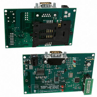
Component Side (Top) Figure 33. NCN6001 Demo Board Printed Circuit Board Layout http://onsemi.com Copper Side (Bottom) Top side 30 ...
Page 31
... Radio Spares 180−8495 Fujitsu FCN−704Q050−AU/M FCI 7434−L01−35S01 CoilCraft 1008PS−223−M Radio Spares 112−2993 ON Semiconductor Radio Spares 203−4910 Radio Spares 203−4910 Radio Spares 203−4910 Radio Spares 203−4910 Radio Spares 203−4910 Radio Spares 203− ...
Page 32
GND GND J5 17 Swa GND 18 18 Swb CRD_DET 7 20 CRD_IO I RST CRD_RST 3 17 CLK CRD_CLK 13 5 GND CRD_VC C4/ C8/S1 ...
Page 33
Table of Contents COMPACT SMART CARD INTERFACE IC MAXIMUM RATINGS . . . . . . . . . . . . . . . . . . . . . . . . . . . . . . ...
Page 34
ABBREVIATIONS Lout_L and Lout_H DC/DC External Inductor Cout Output Capacitor Class A 5V Smart Card Class B 3V Smart Card CRD_C4 Interface IC Card Digital Control CRD_C8 Interface IC Card Digital Control CRD_CLK Interface IC Card Clock Input CRD_DET Card ...
Page 35
... −V− 0.100 (0.004) −T− SEATING PLANE 16X 0.36 *For additional information on our Pb−Free strategy and soldering details, please download the ON Semiconductor Soldering and Mounting Techniques Reference Manual, SOLDERRM/D. PACKAGE DIMENSIONS TSSOP−20 CASE 948E−02 ISSUE Í Í Í Í ...
Page 36
... C 19X NOTE 3 *For additional information on our Pb−Free strategy and soldering details, please download the ON Semiconductor Soldering and Mounting Techniques Reference Manual, SOLDERRM/D. N. American Technical Support: 800−282−9855 Toll Free USA/Canada Europe, Middle East and Africa Technical Support: Phone: 421 33 790 2910 Japan Customer Focus Center Phone: 81− ...