CRD4525-Q1 Cirrus Logic Inc, CRD4525-Q1 Datasheet - Page 4
CRD4525-Q1
Manufacturer Part Number
CRD4525-Q1
Description
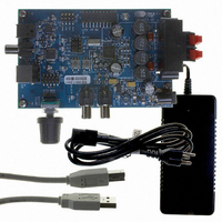
REFERENCE BOARD FOR CS4525 PWM
Manufacturer
Cirrus Logic Inc
Series
Popguard®r
Specifications of CRD4525-Q1
Amplifier Type
Class D
Output Type
2-Channel (Stereo)
Max Output Power X Channels @ Load
15W x 2 @ 8 Ohm
Voltage - Supply
12 V ~ 18 V
Operating Temperature
0°C ~ 70°C
Board Type
Fully Populated
Utilized Ic / Part
CS4525
Lead Free Status / RoHS Status
Contains lead / RoHS non-compliant
Other names
598-1586


4
7. PCB LAYOUT CONSIDERATIONS ..................................................................................................... 65
8. REGISTER QUICK REFERENCE ........................................................................................................ 66
9. REGISTER DESCRIPTIONS ................................................................................................................ 69
6.3 PWM Modulators and Sample Rate Converters ............................................................................ 58
6.4 Output Filters ................................................................................................................................. 59
6.5 Analog Inputs ................................................................................................................................. 61
6.6 Serial Audio Interfaces ................................................................................................................... 62
6.7 Integrated VD Regulator ................................................................................................................ 63
6.8 I²C Control Port Description and Timing ........................................................................................ 64
7.1 Power Supply, Grounding .............................................................................................................. 65
7.2 Output Filter Layout ....................................................................................................................... 65
7.3 QFN Thermal Pad .......................................................................................................................... 65
9.1 Clock Configuration (Address 01h) ................................................................................................ 69
9.2 Input Configuration (Address 02h) ................................................................................................. 71
9.3 AUX Port Configuration (Address 03h) .......................................................................................... 72
9.4 Output Configuration (Address 04h) ............................................................................................. 73
9.5 Foldback and Ramp Configuration (Address 05h) ......................................................................... 74
6.2.3 Input Source Selection .......................................................................................................... 55
6.2.4 PWM Channel Delay ............................................................................................................ 55
6.2.5 Digital Signal Flow ................................................................................................................ 56
6.2.6 Thermal Foldback ................................................................................................................. 57
6.2.7 Automatic Power Stage Shut-Down ..................................................................................... 58
6.4.1 Half-Bridge Output Filter ....................................................................................................... 59
6.4.2 Full-Bridge Output Filter (Stereo or Parallel) ........................................................................ 60
6.6.1 I²S Data Format .................................................................................................................... 62
6.6.2 Left-Justified Data Format .................................................................................................... 62
6.6.3 Right-Justified Data Format .................................................................................................. 63
9.1.1 SYS_CLK Output Enable (EnSysClk) ................................................................................... 69
9.1.2 SYS_CLK Output Divider (DivSysClk) .................................................................................. 69
9.1.3 Clock Frequency (ClkFreq[1:0]) ............................................................................................ 69
9.1.4 HP_Detect/Mute Pin Active Logic Level (HP/MutePol) ......................................................... 70
9.1.5 HP_Detect/Mute Pin Mode (HP/Mute) .................................................................................. 70
9.1.6 Modulator Phase Shifting (PhaseShift) ................................................................................. 70
9.1.7 AM Frequency Shifting (FreqShift) ....................................................................................... 70
9.2.1 Input Source Selection (ADC/SP) ......................................................................................... 71
9.2.2 ADC High-Pass Filter Enable (EnAnHPF) ............................................................................ 71
9.2.3 Serial Port Sample Rate (SPRate[1:0]) - Read Only ............................................................ 71
9.2.4 Input Serial Port Digital Interface Format (DIF [2:0]) ............................................................ 71
9.3.1 Enable Aux Serial Port (EnAuxPort) ..................................................................................... 72
9.3.2 Delay & Warning Port Configuration (DlyPortCfg[1:0]) ......................................................... 72
9.3.3 Aux/Delay Serial Port Digital Interface Format (AuxI²S/LJ) .................................................. 72
9.3.4 Aux Serial Port Right Channel Data Select (RChDSel[1:0]) ................................................. 72
9.3.5 Aux Serial Port Left Channel Data Select (LChDSel[1:0]) .................................................... 73
9.4.1 Output Configuration (OutputCfg[1:0]) .................................................................................. 73
9.4.2 PWM Signals Output Data Select (PWMDSel[1:0]) .............................................................. 73
9.4.3 Channel Delay Settings (OutputDly[3:0]) .............................................................................. 73
9.5.1 Select VP Level (SelectVP) .................................................................................................. 74
9.5.2 Enable Thermal Foldback (EnTherm) ................................................................................... 74
9.5.3 Lock Foldback Adjust (LockAdj) ........................................................................................... 74
9.5.4 Foldback Attack Delay (AttackDly[1:0]) ................................................................................ 75
6.2.2.2 Power-Down Sequence ............................................................................................ 55
6.2.5.1 High-Pass Filter ........................................................................................................ 56
6.2.5.2 Mute Control ............................................................................................................. 56
6.2.5.3 Warning and Error Reporting .................................................................................... 56
CS4525
DS726PP3
Related parts for CRD4525-Q1
Image
Part Number
Description
Manufacturer
Datasheet
Request
R

Part Number:
Description:
Development Kit
Manufacturer:
Cirrus Logic Inc
Datasheet:
Part Number:
Description:
Development Kit
Manufacturer:
Cirrus Logic Inc
Datasheet:


Part Number:
Description:
High-efficiency PFC + Fluorescent Lamp Driver Reference Design
Manufacturer:
Cirrus Logic Inc
Datasheet:
Part Number:
Description:
Development Kit
Manufacturer:
Cirrus Logic Inc
Datasheet:
Part Number:
Description:
Development Kit
Manufacturer:
Cirrus Logic Inc
Datasheet:

Part Number:
Description:
Development Kit
Manufacturer:
Cirrus Logic Inc
Datasheet:
Part Number:
Description:
Development Kit
Manufacturer:
Cirrus Logic Inc
Datasheet:
Part Number:
Description:
Development Kit
Manufacturer:
Cirrus Logic Inc
Datasheet:
Part Number:
Description:
Audio Modules & Development Tools EvalBd 30W Qd Hlf- Brdg Dig Amp Pwr Stg
Manufacturer:
Cirrus Logic Inc
Datasheet:

Part Number:
Description:
EVALUATION BOARD FOR CS8427
Manufacturer:
Cirrus Logic Inc
Datasheet:

Part Number:
Description:
BOARD EVAL FOR CS8416 RCVR
Manufacturer:
Cirrus Logic Inc
Datasheet:

Part Number:
Description:
EVALUATION BOARD FOR CS8420
Manufacturer:
Cirrus Logic Inc
Datasheet:

Part Number:
Description:
KIT DEVELOPMENT EP9315 ARM9
Manufacturer:
Cirrus Logic Inc
Datasheet: