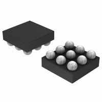
NCP2990FCT2GEVB ON Semiconductor, NCP2990FCT2GEVB Datasheet - Page 3

NCP2990FCT2GEVB
Manufacturer Part Number
NCP2990FCT2GEVB
Description
EVAL BOARD FOR NCP2990FCT2G
Manufacturer
ON Semiconductor
Specifications of NCP2990FCT2GEVB
Design Resources
NCP2990 EVB BOM NCP2990FCT2GEVB Gerber Files NCP2990 EVB Schematic
Amplifier Type
Class AB
Output Type
1-Channel (Mono)
Max Output Power X Channels @ Load
1.35W x 1 @ 8 Ohm
Voltage - Supply
2.2 V ~ 5.5 V
Operating Temperature
-10°C ~ 75°C
Board Type
Fully Populated
Utilized Ic / Part
NCP2990
Lead Free Status / RoHS Status
Lead free / RoHS Compliant
For Use With/related Products
NCP2990FCT2G
Other names
NCP2990FCT2GEVBOS
Stresses exceeding Maximum Ratings may damage the device. Maximum Ratings are stress ratings only. Functional operation above the
Recommended Operating Conditions is not implied. Extended exposure to stresses above the Recommended Operating Conditions may affect
device reliability.
1. Maximum electrical ratings are defined as those values beyond which damage to the device may occur at T
2. The thermal shutdown set to 160°C (typical) avoids irreversible damage on the device due to power dissipation.
3. The R
4. Human Body Model, 100 pF discharge through a 1.5 kW resistor following specification JESD22/A114.
5. Machine Model, 200 pF discharged through all pins following specification JESD22/A115.
PIN DESCRIPTION
MAXIMUM RATINGS
Supply Voltage
Operating Supply Voltage
Input Voltage
Max Output Current
Power Dissipation (Note 2)
Operating Ambient Temperature
Max Junction Temperature
Storage Temperature Range
Thermal Resistance Junction−to−Air
ESD Protection
500 mm
dissipation.
Pin
A1
A2
A3
B1
B2
B3
C1
C2
C3
qJA
2
. For further information see page 10. The bumps have the same thermal resistance and all need to be connected to optimize the power
is highly dependent of the PCB Heatsink area. For example, R
Type
O
O
I
I
I
I
I
I
I
(Note 1)
SHUTDOWN
BYPASS
Symbol
OUTA
OUTB
VM_P
INM
INP
VM
V
p
Rating
Human Body Model (HBM) (Note 4)
Machine Model (MM) (Note 5)
Negative input of the first amplifier, receives the audio input signal. Connected to the
feedback resistor R
Negative output of the NCP2990. Connected to the load and to the feedback resistor Rf.
Positive input of the first amplifier, receives the common mode voltage.
Power Analog Ground.
Core Analog Ground.
Positive analog supply of the cell. Range: 2.2 V−5.5 V.
Bypass capacitor pin which provides the common mode voltage (Vp/2).
Positive output of the NCP2990. Connected to the load.
The device enters in shutdown mode when a low level is applied on this pin.
http://onsemi.com
NCP2990
f
and to the input resistor R
3
qJA
can equal 195°C/W with 50 mm
Symbol
Op Vp
R
Iout
T
Description
V
Pd
V
T
T
stg
qJA
−
in
A
J
p
in
.
2.0 V = Functional Only
Internally Limited
−0.3 to Vcc +0.3
−65 to +150
2.2 to 5.5 V
2
−40 to +85
total area and also 135°C/W with
(Note 3)
A
Value
8000
>250
500
150
= +25°C.
6.0
°C/W
Unit
mA
°C
°C
°C
V
V
V
−
−


