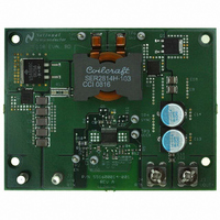
LM5118EVAL/NOPB National Semiconductor, LM5118EVAL/NOPB Datasheet - Page 20

LM5118EVAL/NOPB
Manufacturer Part Number
LM5118EVAL/NOPB
Description
BOARD EVALUATION FOR LM5118
Manufacturer
National Semiconductor
Series
PowerWise®r
Specifications of LM5118EVAL/NOPB
Main Purpose
DC/DC, Step Up or Down
Outputs And Type
1, Non-Isolated
Voltage - Output
12V
Current - Output
3A
Voltage - Input
5 ~ 75V
Regulator Topology
Buck-Boost
Frequency - Switching
300kHz
Board Type
Fully Populated
Utilized Ic / Part
LM5118
Lead Free Status / RoHS Status
Not applicable / Not applicable
Power - Output
-
Other names
*LM5118EVAL
LM5118EVAL
LM5118EVAL
www.national.com
be located close to the RHP zero. The error amplifier zero
(see below) should be placed near the dominate modulator
pole. This is a good starting point for compensation. Refer to
the on-line LM5118 Quick-Start calculator for ready to use
equations and more details.
Components R4 and C18 configure the error amplifier as a
type II configuration which has a DC pole and a zero at
C17 introduces an additional pole used to cancel high fre-
quency switching noise. The error amplifier zero cancels the
modulator pole leaving a single pose response at the
crossover frequency of the loop gain if the crossover frequen-
cy is much lower than the right half plane zero frequency. A
single pole response at the crossover frequency yields a very
stable loop with 90 degrees of phase margin.
For the design example, a target loop bandwidth (crossover
frequency) of 2.0 kHz was selected (about 30% of the right-
FIGURE 14. Error Amplifier Gain and Phase
FIGURE 13. Modulator Gain and Phase
20
half-plane zero frequency). The error amplifier zero (fz)
should be selected at a frequency near that of the modulator
pole and much less than the target crossover frequency. This
constrains the product of R4 and C18 for a desired compen-
sation network zero to be less than 2 kHz. Increasing R4,
while proportionally decreasing C18 increases the error amp
gain. Conversely, decreasing R4 while proportionally increas-
ing C18 decreases the error amp gain. For the design exam-
ple C18 was selected for 4.7 nF and R4 was selected to be
10 kΩ. These values set the compensation network zero at
149 Hz. The overall loop gain can be predicted as the sum (in
dB) of the modulator gain and the error amp gain.
If a network analyzer is available, the modulator gain can be
measured and the error amplifier gain can be configured for
the desired loop transfer function. If a network analyzer is not
available, the error amplifier compensation components can
be designed with the guidelines given. Step load transient
tests can be performed to verify acceptable performance. The
step load goal is minimal overshoot with a damped response.
30058549
30058548


