DAK-85 Power Integrations, DAK-85 Datasheet - Page 2
DAK-85
Manufacturer Part Number
DAK-85
Description
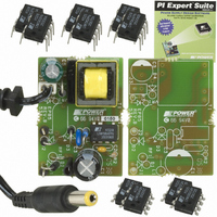
DESIGN ACCELERATOR KIT LP SWITCH
Manufacturer
Power Integrations
Series
LinkSwitch®-LPr
Specifications of DAK-85
Main Purpose
AC/DC, Primary Side
Outputs And Type
1, Isolated
Power - Output
2W
Voltage - Output
6V
Current - Output
330mA
Voltage - Input
90 ~ 265VAC
Regulator Topology
Flyback
Frequency - Switching
66kHz
Board Type
Bare (Unpopulated) and Fully Populated
Utilized Ic / Part
LNK562, LNK563, LNK564
Lead Free Status / RoHS Status
Lead free / RoHS Compliant
Other names
596-1104
Available stocks
Company
Part Number
Manufacturer
Quantity
Price
Company:

Part Number:
DAK-85
Manufacturer:
Power Integrations
Quantity:
135


Rev. H 11/08
Figure 2. Functional Block Diagram.
Pin Functional Description
DRAIN (D) Pin:
The power MOSFET drain connection provides internal
operating current for both startup and steady-state operation.
BYPASS (BP) Pin:
A 0.1 μF external bypass capacitor for the internally generated
5.8 V supply is connected to this pin.
FEEDBACK (FB) Pin:
During normal operation, switching of the power MOSFET is
controlled by this pin. MOSFET switching is disabled when a
current greater than 70 μA fl ows into this pin.
SOURCE (S) Pin:
This pin is the power MOSFET source connection. It is also the
ground reference for the BYPASS and FEEDBACK pins.
LinkSwitch-LP Functional
Description
LinkSwitch-LP comprises a 700 V power MOSFET switch with
a power supply controller on the same die. Unlike conventional
PWM (pulse width modulation) controllers, it uses a simple
ON/OFF control to regulate the output voltage. The controller
consists of an oscillator, feedback (sense and logic) circuit, 5.8
V regulator, BYPASS pin undervoltage circuit, over-temperature
2
OPEN LOOP
PULLDOWN
FEEDBACK
BYPASS
(FB)
(BP)
LNK562-564
0.8 V
1.69 V -V
+
TH
6.3 V
OSCILLATOR
ADJ
JITTER
AUTO-RESTART
RESET
CLOCK
DC
COUNTER
MAX
FAULT
PRESENT
Figure 3. Pin Confi guration.
protection, frequency jittering, current limit circuit, and leading
edge blanking.
Oscillator
The typical oscillator frequency is internally set to an average
of 66/83/100 kHz for the LNK562, 563 & 564 respectively.
Two signals are generated from the oscillator: the maximum
duty cycle signal (DC
the beginning of each switching cycle.
4.85 V
5.8 V
BP
FB
G Package (SMD-8B)
P Package (DIP-8B)
S
S
SHUTDOWN
THERMAL
1
2
3
4
+
-
S
R
Q
Q
BYPASS PIN
UNDER-VOLTAGE
REGULATOR
MAX
8
7
5
5.8 V
) and the clock signal that indicates
S
D
S
CURRENT LIMIT
COMPARATOR
PI-3958-092905
BLANKING
LEADING
EDGE
BP
FB
D
D Package (SO-8C)
+
-
1
2
4
V I
LIMIT
SOURCE
DRAIN
PI-4547-011107
(D)
(S)
8
7
6
5
S
S
S
S
Related parts for DAK-85
Image
Part Number
Description
Manufacturer
Datasheet
Request
R

Part Number:
Description:
KIT DESIGN ACCELERATOR MODEM
Manufacturer:
Power Integrations
Datasheet:

Part Number:
Description:
KIT DESIGN ACCELERATOR SET TOP
Manufacturer:
Power Integrations
Datasheet:

Part Number:
Description:
KIT REF DES DPA 6.6W DC-DC CONV
Manufacturer:
Power Integrations
Datasheet:

Part Number:
Description:
KIT DESIGN ACCELERATOR POE CONV
Manufacturer:
Power Integrations
Datasheet:

Part Number:
Description:
DESIGN ACCELERATOR KIT XT SWITCH
Manufacturer:
Power Integrations
Datasheet:

Part Number:
Description:
KIT DESIGN ACC PEAKSWITCH FAMILY
Manufacturer:
Power Integrations
Datasheet:

Part Number:
Description:
KIT DESIGN ACCELERATOR ADAPTER
Manufacturer:
Power Integrations
Datasheet:

Part Number:
Description:
KIT DESIGN ACCELERATOR ADAPTER
Manufacturer:
Power Integrations
Datasheet:

Part Number:
Description:
KIT DESIGN ACCELERATOR DC-DC
Manufacturer:
Power Integrations
Datasheet:

Part Number:
Description:
KIT DESIGN ACCELERATOR DPA SW
Manufacturer:
Power Integrations
Datasheet: