551011367-051 National Semiconductor, 551011367-051 Datasheet - Page 25
551011367-051
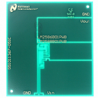
Manufacturer Part Number
551011367-051
Description
BOARD WEBENCH BUILD IT LM2586/88
Manufacturer
National Semiconductor
Series
WEBENCH® Buildit Boardr
Specifications of 551011367-051
Main Purpose
DC/DC, Step Up
Regulator Topology
Boost
Board Type
Bare (Unpopulated)
Utilized Ic / Part
LM2586, LM2588
Lead Free Status / RoHS Status
Not applicable / Not applicable
Current - Output
-
Voltage - Output
-
Voltage - Input
-
Power - Output
-
Frequency - Switching
-
Outputs And Type
-
Lead Free Status / Rohs Status
Not Compliant
Other names
*551011367-051


Application Hints
FREQUENCY SYNCHRONIZATION
Another feature of the LM2586 is the ability to synchronize
the switching frequency to an external source, using the
sync pin (pin 6). This feature allows the user to parallel
multiple devices to deliver more output power.
A negative falling pulse applied to the sync pin will synchro-
nize the LM2586 to an external oscillator (see Figures 40,
41).
PROGRAMMING OUTPUT VOLTAGE
(SELECTING R1 AND R2)
Referring to the adjustable regulator in Figure 42, the output
voltage is programmed by the resistors R1 and R2 by the
following formula:
Resistors R1 and R2 divide the output voltage down so that
it can be compared with the 1.23V internal reference. With
R2 between 1k and 5k, R1 is:
V
R1 = R2 (V
OUT
FIGURE 39. Frequency Setting Resistor Guide
FIGURE 40. Frequency Synchronization
= V
REF
R
OUT
SET
Open
200
47
33
22
(1 + R1/R2)
/V
(kΩ)
REF
− 1)
Frequency (kHz)
(Continued)
100
125
150
175
200
where V
where V
REF
REF
FIGURE 42. Boost Regulator
= 1.23V
= 1.23V
01251659
25
Use of this feature enables the LM2586 to be synchronized
to an external oscillator, such as a system clock. This opera-
tion allows multiple power supplies to operate at the same
frequency, thus eliminating frequency-related noise prob-
lems.
The scope photo in Figure 41 shows a LM2586 12V Boost
Regulator synchronized to a 200 kHz signal. There is a 700
ns delay between the falling edge of the sync signal and the
turning on of the switch.
For best temperature coefficient and stability with time, use
1% metal film resistors.
SHORT CIRCUIT CONDITION
Due to the inherent nature of boost regulators, when the
output is shorted (see Figure 42), current flows directly from
the input, through the inductor and the diode, to the output,
bypassing the switch. The current limit of the switch does not
limit the output current for the entire circuit. To protect the
load and prevent damage to the switch, the current must be
externally limited, either by the input supply or at the output
FIGURE 41. Waveforms of a Synchronized
12V Boost Regulator
01251661
www.national.com
01251669
Related parts for 551011367-051
Image
Part Number
Description
Manufacturer
Datasheet
Request
R

Part Number:
Description:
BERGSTIK-0.100 TH R/A TIN
Manufacturer:
FCI
Datasheet:
Part Number:
Description:
BERGSTIK 0.100" R/A TH 15 GOLD
Manufacturer:
FCI
Datasheet:
Part Number:
Description:
BERGSTIK 0.100 TH R/A 30GOLD
Manufacturer:
FCI
Datasheet:
Part Number:
Description:
BERGSTIK 0.100" R/A TH 15 GOLD
Manufacturer:
FCI
Datasheet:
Part Number:
Description:
BERGSTIK 0.100" R/A TH 30 GOLD
Manufacturer:
FCI
Datasheet:
Part Number:
Description:
BERGSTIK-0.100 TH R/A TIN
Manufacturer:
FCI
Datasheet:
Part Number:
Description:
BERGSTIK 0.100" R/A TH 30 GOLD
Manufacturer:
FCI
Datasheet:
Part Number:
Description:
BERGSTIK 0.100" R/A TH 30 GOLD
Manufacturer:
FCI
Datasheet:
Part Number:
Description:
BERGSTIK 0.100 TH R/A 30GOLD
Manufacturer:
FCI
Datasheet:
Part Number:
Description:
BERGSTIK 0.100 TH R/A 15 GOLD
Manufacturer:
FCI
Datasheet:

Part Number:
Description:
National Semiconductor [8-Bit D/A Converter]
Manufacturer:
National Semiconductor
Datasheet:
Part Number:
Description:
National Semiconductor [Media Coprocessor]
Manufacturer:
National Semiconductor
Datasheet:
Part Number:
Description:
Digitally Controlled Tone and Volume Circuit with Stereo Audio Power Amplifier, Microphone Preamp Stage and National 3D Sound
Manufacturer:
National Semiconductor
Datasheet:
Part Number:
Description:
Digitally Controlled Tone and Volume Circuit with Stereo Audio Power Amplifier, Microphone Preamp Stage and National 3D Sound
Manufacturer:
National Semiconductor
Datasheet:
Part Number:
Description:
AC97 Rev 2 Codec with Sample Rate Conversion and National 3D Sound
Manufacturer:
National Semiconductor