551011367-051 National Semiconductor, 551011367-051 Datasheet - Page 28
551011367-051
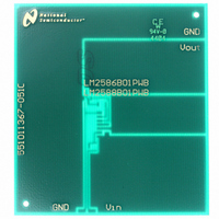
Manufacturer Part Number
551011367-051
Description
BOARD WEBENCH BUILD IT LM2586/88
Manufacturer
National Semiconductor
Series
WEBENCH® Buildit Boardr
Specifications of 551011367-051
Main Purpose
DC/DC, Step Up
Regulator Topology
Boost
Board Type
Bare (Unpopulated)
Utilized Ic / Part
LM2586, LM2588
Lead Free Status / RoHS Status
Not applicable / Not applicable
Current - Output
-
Voltage - Output
-
Voltage - Input
-
Power - Output
-
Frequency - Switching
-
Outputs And Type
-
Lead Free Status / Rohs Status
Not Compliant
Other names
*551011367-051


www.national.com
Application Hints
indicated in Figure 45). When using the Adjustable version,
physically locate the programming resistors as near the
regulator IC as possible, to keep the sensitive feedback
wiring short.
HEAT SINK/THERMAL CONSIDERATIONS
In many cases, a heat sink is not required to keep the
LM2586 junction temperature within the allowed operating
temperature range. For each application, to determine
whether or not a heat sink will be required, the following must
be identified:
1) Maximum ambient temperature (in the application).
2) Maximum regulator power dissipation (in the application).
3) Maximum allowed junction temperature (125˚C for the
LM2586). For a safe, conservative design, a temperature
approximately 15˚C cooler than the maximum junction tem-
perature should be selected (110˚C).
4) LM2586 package thermal resistances θ
in the Electrical Characteristics).
Total power dissipated (P
as follows:
V
N is the transformer turns ratio, D is the duty cycle, and I
is the maximum load current (and
maximum load currents for multiple-output flyback regula-
tors). The duty cycle is given by:
where V
typically 0.5V for Schottky diodes and 0.8V for fast recovery
diodes. V
found in the Characteristic Curves.
When no heat sink is used, the junction temperature rise is:
IN
is the minimum input voltage, V
F
SAT
is the forward biased voltage of the diode and is
is the switch saturation voltage and can be
∆T
J
D
) by the LM2586 can be estimated
= P
D
(Continued)
• θ
OUT
∑
JA
I
.
LOAD
is the output voltage,
JA
is the sum of the
and θ
JC
(given
LOAD
28
Adding the junction temperature rise to the maximum ambi-
ent temperature gives the actual operating junction tempera-
ture:
If the operating junction temperature exceeds the maximum
junction temperatue in item 3 above, then a heat sink is
required. When using a heat sink, the junction temperature
rise can be determined by the following:
Again, the operating junction temperature will be:
As before, if the maximum junction temperature is exceeded,
a larger heat sink is required (one that has a lower thermal
resistance).
Included in the Switchers Made Simple
a more precise (non-linear) thermal model that can be used
to determine junction temperature with different input-output
parameters or different component values. It can also calcu-
late the heat sink thermal resistance required to maintain the
regulator junction temperature below the maximum operat-
ing temperature.
To further simplify the flyback regulator design procedure,
National Semiconductor is making available computer de-
sign software to be used with the Simple Switcher
switching regulators. Switchers Made Simple is available
on a 3
National Semiconductor sales office in your area or the
National
(1-800-272-9959).
1
⁄
2
" diskette for IBM compatible computers from a
∆T
Semiconductor
J
= P
D
• (θ
T
T
J
JC
J
= ∆T
= ∆T
+ θ
Customer
Interface
J
J
+ T
+ T
A
A
.
+ θ
®
Response
Heat Sink
design software is
)
®
Center
line of
Related parts for 551011367-051
Image
Part Number
Description
Manufacturer
Datasheet
Request
R

Part Number:
Description:
BERGSTIK-0.100 TH R/A TIN
Manufacturer:
FCI
Datasheet:
Part Number:
Description:
BERGSTIK 0.100" R/A TH 15 GOLD
Manufacturer:
FCI
Datasheet:
Part Number:
Description:
BERGSTIK 0.100 TH R/A 30GOLD
Manufacturer:
FCI
Datasheet:
Part Number:
Description:
BERGSTIK 0.100" R/A TH 15 GOLD
Manufacturer:
FCI
Datasheet:
Part Number:
Description:
BERGSTIK 0.100" R/A TH 30 GOLD
Manufacturer:
FCI
Datasheet:
Part Number:
Description:
BERGSTIK-0.100 TH R/A TIN
Manufacturer:
FCI
Datasheet:
Part Number:
Description:
BERGSTIK 0.100" R/A TH 30 GOLD
Manufacturer:
FCI
Datasheet:
Part Number:
Description:
BERGSTIK 0.100" R/A TH 30 GOLD
Manufacturer:
FCI
Datasheet:
Part Number:
Description:
BERGSTIK 0.100 TH R/A 30GOLD
Manufacturer:
FCI
Datasheet:
Part Number:
Description:
BERGSTIK 0.100 TH R/A 15 GOLD
Manufacturer:
FCI
Datasheet:

Part Number:
Description:
National Semiconductor [8-Bit D/A Converter]
Manufacturer:
National Semiconductor
Datasheet:
Part Number:
Description:
National Semiconductor [Media Coprocessor]
Manufacturer:
National Semiconductor
Datasheet:
Part Number:
Description:
Digitally Controlled Tone and Volume Circuit with Stereo Audio Power Amplifier, Microphone Preamp Stage and National 3D Sound
Manufacturer:
National Semiconductor
Datasheet:
Part Number:
Description:
Digitally Controlled Tone and Volume Circuit with Stereo Audio Power Amplifier, Microphone Preamp Stage and National 3D Sound
Manufacturer:
National Semiconductor
Datasheet:
Part Number:
Description:
AC97 Rev 2 Codec with Sample Rate Conversion and National 3D Sound
Manufacturer:
National Semiconductor