LM5030EVAL National Semiconductor, LM5030EVAL Datasheet - Page 7
LM5030EVAL
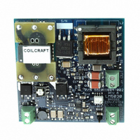
Manufacturer Part Number
LM5030EVAL
Description
EVALUATION BOARD FOR LM5030
Manufacturer
National Semiconductor
Series
PowerWise®r
Specifications of LM5030EVAL
Main Purpose
DC/DC, Step Down
Outputs And Type
1, Isolated
Voltage - Output
3.3V
Current - Output
10A
Voltage - Input
36 ~ 75V
Regulator Topology
Buck
Board Type
Fully Populated
Utilized Ic / Part
LM5030
Lead Free Status / RoHS Status
Not applicable / Not applicable
Power - Output
-
Frequency - Switching
-
Other names
*LM5030EVAL


Typical Performance Characteristics
Detailed Operating Description
The LM5030 High Voltage PWM controller contains all of the
features needed to implement Push-Pull and Bridge topolo-
gies, using current-mode control in a small 10 pin package.
Features included are, startup regulator, dual mode current
limit, dual alternating gate drivers, thermal shutdown, soft-
start and slope compensation. This high speed IC has total
propagation delays
of the LM5030 is shown in Figure 1.
The LM5030 is designed for Current-Mode Control convert-
ers which require alternating outputs, such as Push-Pull and
Half/Full Bridge topologies. The features included in the
LM5030 enable all of the advantages of Current-Mode Con-
trol, line feed-forward, cycle by cycle current limit and sim-
plified loop compensation. The oscillator ramp is internally
buffered and added to the PWM comparator input to provide
slope compensation necessary for current mode control at
higher duty cycles.
High Voltage Start-Up Regulator
The LM5030 contains an internal high voltage startup regu-
lator. The input pin (Vin) can be connected directly to line
voltages as high as 100V. The regulator output is internally
current limited to 10mA. Upon power up, the regulator is
enabled and sources current into an external capacitor con-
nected to the V
for the V
the V
ler outputs are enabled. The outputs will remain enabled
unless, V
pulled to ground or an over temperature condition occurs. In
typical applications, an auxiliary transformer winding is diode
connected to the V
voltage greater than 8V, effectively shutting off the internal
startup regulator and saving power while reducing the con-
troller dissipation. The external V
such that the self-bias will maintain a V
than 6.1V during the initial start-up. During a fault mode
when the converter self bias winding is inactive, external
current draw on the V
exceed the maximum power dissipation of the controller. An
external start-up or other bias rail can be used instead of the
internal start-up regulator by connecting the V
pins and feeding the external bias voltage (8 - 15V) to that
node.
CC
pin reaches the regulation point of 7.7V, the control-
CC
CC
regulator is 0.1µF to 50µF. When the voltage on
falls below 6.1V or if the SS/SHUTDOWN pin is
Feedback Amplifier Gainphase
CC
pin. The recommended capacitance range
<
CC
100nS. The Functional Block Diagram
CC
pin. This winding raises the V
line should be limited as to not
CC
capacitor must be sized
CC
voltage greater
CC
and the Vin
20058115
CC
Unless otherwise specified: T
7
Error Amplifier
An internal high gain error amplifier is provided within the
LM5030. The amplifier’s non-inverting reference is tied to
1.25V. In non-isolated applications the power converter out-
put is connected to the VFB pin via the voltage setting
resistors and loop compensation is connected between the
COMP and VFB pins.
For most isolated applications the error amplifier function is
implemented on the secondary side ground. Since the inter-
nal error amplifier is configured as an open drain output it
can be disabled by connecting VFB to ground. The internal
5K pull-up resistor, connected between the 5V reference and
COMP, can be used as the pull-up for an optocoupler or
other isolation device.
PWM Comparator
The PWM comparator compares the compensated current
ramp signal to the loop error voltage from the internal error
amplifier (COMP pin). This comparator is optimized for
speed in order to achieve minimum discernable duty cycles.
The comparator polarity is such that zero Volts on the COMP
pin will cause a zero duty cycle.
Current Limit/ Current Sense
The LM5030 contains two levels of over-current protection. If
the voltage on the current sense comparator exceeds 0.5
Volts the present cycle is terminated (cycle by cycle current
limit). If the voltage on the current sense comparator ex-
ceeds 0.625 Volts, the controller will terminate the present
cycle and discharge the softstart capacitor. A small RC filter,
located near the controller, is recommended for the CS pin.
An internal MOSFET discharges the current sense filter
capacitor at the conclusion of every cycle, to improve dy-
namic performance.
The LM5030 CS and PWM comparators are very fast, and
as such will respond to short duration noise pulses. Layout
considerations are critical for the current sense filter and
sense resistor. The capacitor associated with the CS filter
must be placed very close to the device and connected
directly to the pins of the IC (CS and RTN). Also if a current
sense transformer is used, both leads of the transformer
secondary should be routed to the sense resistor, which
should also be located close to the IC. If a current sense
resistor located in the drive transistor sources is used, for
current sense, a low inductance resistor should be chosen.
J
= 25˚C. (Continued)
www.national.com
Related parts for LM5030EVAL
Image
Part Number
Description
Manufacturer
Datasheet
Request
R

Part Number:
Description:
National Semiconductor [8-Bit D/A Converter]
Manufacturer:
National Semiconductor
Datasheet:
Part Number:
Description:
National Semiconductor [Media Coprocessor]
Manufacturer:
National Semiconductor
Datasheet:
Part Number:
Description:
Digitally Controlled Tone and Volume Circuit with Stereo Audio Power Amplifier, Microphone Preamp Stage and National 3D Sound
Manufacturer:
National Semiconductor
Datasheet:
Part Number:
Description:
Digitally Controlled Tone and Volume Circuit with Stereo Audio Power Amplifier, Microphone Preamp Stage and National 3D Sound
Manufacturer:
National Semiconductor
Datasheet:
Part Number:
Description:
AC97 Rev 2 Codec with Sample Rate Conversion and National 3D Sound
Manufacturer:
National Semiconductor
Part Number:
Description:
Manufacturer:
National Semiconductor
Datasheet:
Part Number:
Description:
Manufacturer:
National Semiconductor
Datasheet:
Part Number:
Description:
General Purpose, Low Voltage, Low Power, Rail-to-Rail Output Operational Amplifiers
Manufacturer:
National Semiconductor
Datasheet:
Part Number:
Description:
8-bit 20 MSPS flash A/D converter.
Manufacturer:
National Semiconductor
Datasheet:
Part Number:
Description:
Low Noise Quad Operational Amplifier
Manufacturer:
National Semiconductor
Datasheet:
Part Number:
Description:
Quad Differential Line Receivers
Manufacturer:
National Semiconductor
Datasheet:
Part Number:
Description:
Quad High Speed Trapezoidal? Bus Transceiver
Manufacturer:
National Semiconductor
Datasheet:
Part Number:
Description:
Dual Line Receiver
Manufacturer:
National Semiconductor
Datasheet:
Part Number:
Description:
TTL to 10k ECL Level Translator with Latch
Manufacturer:
National Semiconductor
Datasheet: