NCP5425SOEVB ON Semiconductor, NCP5425SOEVB Datasheet
NCP5425SOEVB
Specifications of NCP5425SOEVB


Related parts for NCP5425SOEVB

NCP5425SOEVB Summary of contents
Page 1
NCP5425 Dual Synchronous Buck Controller The NCP5425 is a highly flexible dual buck controller with internal gate drivers that can be used with two input power supplies and one or two outputs in multiple configurations. The part contains all the ...
Page 2
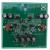
V 3 220 mF C6 0 NTD60N02R NTD110N02RT4 1 680 mF1 R3 0 ...
Page 3
MAXIMUM RATINGS Operating Junction Temperature Storage Temperature Range ESD Susceptibility (Human Body Model) ESD Susceptibility (Machine Model) Thermal Resistance, Junction−to−Air Moisture Sensitivity Level (MSL) Lead Temperature Soldering: Reflow: (Note 1) Stresses exceeding Maximum Ratings may damage ...
Page 4
ELECTRICAL CHARACTERISTICS 10.8 V < BST < GATE(H)1,2 GATE(L)1,2 Characteristic ERROR AMPLIFIER V Input Bias Current FB1 Input Bias Current FB2 REF2 Common Mode Input Voltage Range COMP1(2) Source Current COMP1(2) Sink ...
Page 5
ELECTRICAL CHARACTERISTICS (continued) (0°C < T < 13.2 V; 10.8 V < BST < GATE(H)1,2 Characteristic OSCILLATOR Switching Frequency Switching Frequency Switching Frequency R Voltage OSC Phase Difference Low Noise Disable OVERCURRENT PROTECTION OVC Comparator Offset Voltage ...
Page 6
PIN FUNCTION DESCRIPTION Pin No. Symbol 1 GATE(H)1 High Side Switch FET driver pin for the channel 1 FET. 2 GATE(L)1 Low Side Synchronous FET driver pin for the channel 1 FET. 3 GND Ground. All circuits are referenced to ...
Page 7
IRAMP1 IRAMP2 OSCILLATOR AND CLK1 R RAMP OSC CURRENT CLK2 GENERATOR LNDM Low noise disable mode (pull R OSC 3.1 V REFERENCE AND BIAS 0.8 V 3.1 V − V FB1 + 0.8 V EA1 + − COMP1 − V ...
Page 8
APPLICATIONS INFORMATION Theory of Operation The NCP5425 is a very versatile buck controller using control method. It can be configured as • Dual output Buck Controller. • Two phase Buck Controller with current limit. • Two phase ...
Page 9
COMP pin voltage, minus the 0.3 V PWM comparator offset threshold and the artificial ramp, the PWM comparator terminates the initial pulse. 4.2 V 0.3 V UVLO STARTUP NORMAL OPERATION t s Figure 4. Idealized Startup ...
Page 10
Current Sharing When used in a two separate input to a single output mode, the NCP5425 dual controller can provide input power sharing in either of two ways: • A preset ratio. For example, Channel 1 could provide 70% of ...
Page 11
Inductor Current Sensing Examples of lossless current sensing across an output inductor are shown in Figure the output inductance and Rx represents its equivalent series resistance. To compensate the current sense signal, the values of R1 and ...
Page 12
Figure 8A − Basic Current Sensing Represents a basic inductor sensing configuration. When the voltage at pin +Is exceeds the voltage at pin – (nominal), the internal current sense comparator offset will be overcome. For this case, ...
Page 13
DESIGN GUIDELINES General The output voltage tolerance can be affected by any or all of the following: 1. Buck regulator output voltage set point accuracy. 2. Output voltage change due to discharging or charging of the bulk decoupling capacitors during ...
Page 14
Output Inductor Selection The inductor should be selected based on the criteria of inductance, current capability, and DC resistance. Increasing the inductor value will decrease output voltage ripple, but degrade transient response. There are many factors to consider in selecting ...
Page 15
Maximum allowable ESR can then be determined according to the formula: DV ESR ESR MAX + DI OUT where: DV =change in output voltage due to ESR ESR (assigned by the designer) Once the maximum allowable ESR is determined, the ...
Page 16
I = maximum switching MOSFET RMS current; RMS( inductor peak current; L(PEAK inductor valley current; L(VALLEY duty cycle. Once the RMS current through the switch is known, the switching MOSFET conduction losses can ...
Page 17
Control IC Power Dissipation The power dissipation of the IC varies with the MOSFETs used, VCC, and the NCP5425 operating frequency. The average MOSFET gate charge current typically dominates the control IC power dissipation, and is given by: P CONTROL(IC) ...
Page 18
Given an ESR value of 3.5 mW, the current limit becomes increased current limit is required, a resistor divider can be added (see Figure 8). Advantages of setting the current limit by using the winding resistance ...
Page 19
The values of R2 and R3 can be found by solving two simultaneous equations (R2 * R3) (R2 ) R3) Solving for R2 and R3 yields 1.5R1 R3 + 3R1 Example 2 ...
Page 20
Grounding the Mode pin enables an internal clamp to limit the Comp 2 voltage excursions during overcurrent faults. Without this clamp, the output voltage (Vout1 and Vout2) can overshoot the regulated output voltages when the fault is removed. For a ...
Page 21
EMI MANAGEMENT As a consequence of large currents being turned on and off at high frequency, switching regulators generate noise during normal operation. When designing for compliance with EMI/EMC regulations, additional components may be necessary to reduce noise emissions. These ...
Page 22
... Opportunity/Affirmative Action Employer. This literature is subject to all applicable copyright laws and is not for resale in any manner. PUBLICATION ORDERING INFORMATION LITERATURE FULFILLMENT: Literature Distribution Center for ON Semiconductor P.O. Box 5163, Denver, Colorado 80217 USA Phone: 303−675−2175 or 800−344−3860 Toll Free USA/Canada Fax: 303− ...