NCP5425SOEVB ON Semiconductor, NCP5425SOEVB Datasheet - Page 11
NCP5425SOEVB
Manufacturer Part Number
NCP5425SOEVB
Description
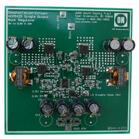
EVAL BOARD FOR NCP5425SO
Manufacturer
ON Semiconductor
Specifications of NCP5425SOEVB
Design Resources
NCP5425SOEVB BOM NCP5425SOEVB Gerber Files NCP5425SOEVB Schematic
Main Purpose
DC/DC, Step Down
Outputs And Type
1, Non-Isolated
Voltage - Output
0.8V
Current - Output
30A
Voltage - Input
4.6 ~ 12 V
Regulator Topology
Buck
Frequency - Switching
300kHz
Board Type
Fully Populated
Utilized Ic / Part
NCP5425
Lead Free Status / RoHS Status
Lead free / RoHS Compliant
Power - Output
-
Lead Free Status / Rohs Status
Lead free / RoHS Compliant
For Use With/related Products
NCP5425SO
Other names
NCP5425SOEVBOS


Inductor Current Sensing
inductor are shown in Figure 8. Lx is the output inductance
and Rx represents its equivalent series resistance. To
compensate the current sense signal, the values of R1 and C1
are chosen so that Lx/Rx = R1 x C1. With these values, the
Examples of lossless current sensing across an output
Output
Output
DC
Rx
Rx
DC
Switch
Switch
Node
Node
Lx
Lx
R1
C1
R1
C1
R3
(8A)
Rx X I
Rx X I
(8C)
−
−
+
+
L
L
Figure 8. Inductor Current Sensing − Circuit Configurations
+ls
−ls
+ls
−ls
_
_
70 mV
70 mV
+
+
http://onsemi.com
NCP5425
11
Output
current sense signal will have the same wave shape as the
inductor current and the voltage signal on C1 will represent
the instantaneous value of inductor current. The voltage
across C1 can be used as though it were a sense resistor with
the same value as the inductor’s ESR, thus avoiding a sense
resistor’s power loss.
DC
Rx
Output
Switch
Node
DC
Rx
Switch
Lx
Node
Lx
C1
R1
(8D)
R1
C1
R2
R3
(Rx*I
(8B)
(R1 + R2)
Rx*I
R4
L
L
−
) + (E
+
*R2
−
+
+ls
−ls
+ls
−ls
R3
E
R3
)
_
_
70 mV
70 mV
= (Vo*R3)/R3 + R4)
+
+
Related parts for NCP5425SOEVB
Image
Part Number
Description
Manufacturer
Datasheet
Request
R

Part Number:
Description:
Dual Synchronous Buck Controller
Manufacturer:
ON Semiconductor
Datasheet:
Part Number:
Description:
ON Semiconductor [VOLTAGE REGULATOR]
Manufacturer:
ON Semiconductor
Datasheet:
Part Number:
Description:
357-036-542-201 CARDEDGE 36POS DL .156 BLK LOPRO
Manufacturer:
ON Semiconductor
Datasheet:
Part Number:
Description:
357-036-542-201 CARDEDGE 36POS DL .156 BLK LOPRO
Manufacturer:
ON Semiconductor
Datasheet:
Part Number:
Description:
357-036-542-201 CARDEDGE 36POS DL .156 BLK LOPRO
Manufacturer:
ON Semiconductor
Datasheet:
Part Number:
Description:
357-036-542-201 CARDEDGE 36POS DL .156 BLK LOPRO
Manufacturer:
ON Semiconductor
Datasheet:
Part Number:
Description:
357-036-542-201 CARDEDGE 36POS DL .156 BLK LOPRO
Manufacturer:
ON Semiconductor
Datasheet:
Part Number:
Description:
357-036-542-201 CARDEDGE 36POS DL .156 BLK LOPRO
Manufacturer:
ON Semiconductor
Datasheet:
Part Number:
Description:
357-036-542-201 CARDEDGE 36POS DL .156 BLK LOPRO
Manufacturer:
ON Semiconductor
Datasheet:
Part Number:
Description:
357-036-542-201 CARDEDGE 36POS DL .156 BLK LOPRO
Manufacturer:
ON Semiconductor
Datasheet:
Part Number:
Description:
357-036-542-201 CARDEDGE 36POS DL .156 BLK LOPRO
Manufacturer:
ON Semiconductor
Datasheet:
Part Number:
Description:
357-036-542-201 CARDEDGE 36POS DL .156 BLK LOPRO
Manufacturer:
ON Semiconductor
Datasheet:
Part Number:
Description:
Manufacturer:
ON Semiconductor
Datasheet:
Part Number:
Description:
Manufacturer:
ON Semiconductor
Datasheet: