NCP5425SOEVB ON Semiconductor, NCP5425SOEVB Datasheet - Page 7
NCP5425SOEVB
Manufacturer Part Number
NCP5425SOEVB
Description
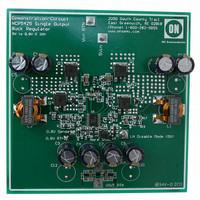
EVAL BOARD FOR NCP5425SO
Manufacturer
ON Semiconductor
Specifications of NCP5425SOEVB
Design Resources
NCP5425SOEVB BOM NCP5425SOEVB Gerber Files NCP5425SOEVB Schematic
Main Purpose
DC/DC, Step Down
Outputs And Type
1, Non-Isolated
Voltage - Output
0.8V
Current - Output
30A
Voltage - Input
4.6 ~ 12 V
Regulator Topology
Buck
Frequency - Switching
300kHz
Board Type
Fully Populated
Utilized Ic / Part
NCP5425
Lead Free Status / RoHS Status
Lead free / RoHS Compliant
Power - Output
-
Lead Free Status / Rohs Status
Lead free / RoHS Compliant
For Use With/related Products
NCP5425SO
Other names
NCP5425SOEVBOS


COMP1
COMP2
V
R
V
V
REF2
V
OSC
FB1
FB2
CC
OSCILLATOR
GENERATOR
REFERENCE
CURRENT
AND BIAS
RAMP
+
−
AND
+
4.2 V
4.0 V
−
−
+
UVLO
0.8 V
IRAMP1
IRAMP2
CLK1
CLK2
LNDM
3.1 V
0.8 V
Low noise disable mode
(pull R
3.1 V
3.1 V
+
+
−
−
OSC
EA1
EA2
high to activate)
UVLO
UVLO
REFERENCE
−
−
+
+
COMP2
CLAMP
Figure 2. Block Diagram
http://onsemi.com
COMP1 CLAMP
REFERENCE
RAMP1
RAMP2
NCP5425
+
+
3.1 V
7
or dual
Single
output
mode
S/D
0.3 V
0.3 V
+
+
−
−
−
−
PWM
COMP1
PWM
COMP2
3.1 V
RAMP1
3.1 V
CLK1
CLK2
MODE
3.1 V
R
R
S
S
Dominant
Dominant
RAMP2
Reset
Reset
IRAMP1
Q
Q
Q
Q
3.1 V
OC1
OC2
IRAMP2
LNDM
LNDM
LNDM
LNDM
−
−
+
+
70 mV
70 mV
BST
V
V
+
+
CC
CC
−
−
BST
IS+1
IS−1
IS+2
IS−2
GATE(H)2
GATE(H)1
GATE(L)1
GATE(L)2
GND
Related parts for NCP5425SOEVB
Image
Part Number
Description
Manufacturer
Datasheet
Request
R

Part Number:
Description:
Dual Synchronous Buck Controller
Manufacturer:
ON Semiconductor
Datasheet:
Part Number:
Description:
ON Semiconductor [VOLTAGE REGULATOR]
Manufacturer:
ON Semiconductor
Datasheet:
Part Number:
Description:
357-036-542-201 CARDEDGE 36POS DL .156 BLK LOPRO
Manufacturer:
ON Semiconductor
Datasheet:
Part Number:
Description:
357-036-542-201 CARDEDGE 36POS DL .156 BLK LOPRO
Manufacturer:
ON Semiconductor
Datasheet:
Part Number:
Description:
357-036-542-201 CARDEDGE 36POS DL .156 BLK LOPRO
Manufacturer:
ON Semiconductor
Datasheet:
Part Number:
Description:
357-036-542-201 CARDEDGE 36POS DL .156 BLK LOPRO
Manufacturer:
ON Semiconductor
Datasheet:
Part Number:
Description:
357-036-542-201 CARDEDGE 36POS DL .156 BLK LOPRO
Manufacturer:
ON Semiconductor
Datasheet:
Part Number:
Description:
357-036-542-201 CARDEDGE 36POS DL .156 BLK LOPRO
Manufacturer:
ON Semiconductor
Datasheet:
Part Number:
Description:
357-036-542-201 CARDEDGE 36POS DL .156 BLK LOPRO
Manufacturer:
ON Semiconductor
Datasheet:
Part Number:
Description:
357-036-542-201 CARDEDGE 36POS DL .156 BLK LOPRO
Manufacturer:
ON Semiconductor
Datasheet:
Part Number:
Description:
357-036-542-201 CARDEDGE 36POS DL .156 BLK LOPRO
Manufacturer:
ON Semiconductor
Datasheet:
Part Number:
Description:
357-036-542-201 CARDEDGE 36POS DL .156 BLK LOPRO
Manufacturer:
ON Semiconductor
Datasheet:
Part Number:
Description:
Manufacturer:
ON Semiconductor
Datasheet:
Part Number:
Description:
Manufacturer:
ON Semiconductor
Datasheet: