DAK-71A Power Integrations, DAK-71A Datasheet - Page 2
DAK-71A
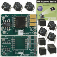
Manufacturer Part Number
DAK-71A
Description
KIT DESIGN ACCELERATOR DC-DC
Manufacturer
Power Integrations
Series
DPA-Switch®r
Specifications of DAK-71A
Main Purpose
DC/DC, Step Down
Outputs And Type
1, Isolated
Voltage - Output
3.3V
Current - Output
2A
Voltage - Input
36 ~ 72V
Regulator Topology
Flyback
Frequency - Switching
400kHz
Board Type
Bare (Unpopulated) and Fully Populated
Utilized Ic / Part
DPA423, DPA424, DPA425
Lead Free Status / RoHS Status
Not applicable / Not applicable
Power - Output
-
Lead Free Status / Rohs Status
Lead free / RoHS Compliant
Other names
596-1009


Rev. S 12/07
Functional Block Diagram ....................................................................................................................................... 3
Pin Functional Description ...................................................................................................................................... 3
DPA-Switch Family Functional Description ............................................................................................................ 4
Using Feature Pins ..................................................................................................................................................... 8
Typical Uses of FREQUENCY (F) Pin ...................................................................................................................... 11
Typical Uses of LINE-SENSE (L) and EXTERNAL CURRENT LIMIT (X) Pins ....................................................... 11
Application Examples .............................................................................................................................................. 14
Key Application Considerations .............................................................................................................................. 16
Product Specifi cations and Test Conditions .......................................................................................................... 21
Typical Performance Characteristics .................................................................................................................. 27
Part Ordering Information ....................................................................................................................................... 30
Package Outlines .................................................................................................................................................... 31
2
CONTROL (C) Pin Operation .................................................................................................................................... 4
Oscillator and Switching Frequency .......................................................................................................................... 5
Pulse Width Modulator & Maximum Duty Cycle ........................................................................................................ 5
Minimum Duty Cycle and Cycle Skipping ................................................................................................................. 6
Error Amplifi er .......................................................................................................................................................... 6
On-chip Current Limit with External Programmability ................................................................................................ 6
Line Under-Voltage Detection (UV) ............................................................................................................................ 6
Line Overvoltage Shutdown (OV) .............................................................................................................................. 6
Line Feed-Forward with DC
Remote ON/OFF ...................................................................................................................................................... 7
Synchronization ........................................................................................................................................................ 7
Soft-Start ................................................................................................................................................................. 8
Shutdown/Auto-Restart ........................................................................................................................................... 8
Hysteretic Over-Temperature Protection ................................................................................................................... 8
Bandgap Reference ................................................................................................................................................. 8
High-Voltage Bias Current Source ............................................................................................................................ 8
FREQUENCY (F) Pin Operation ................................................................................................................................ 8
LINE-SENSE (L) Pin Operation ................................................................................................................................. 9
EXTERNAL CURRENT LIMIT (X) Pin Operation ......................................................................................................... 9
DPA-Switch Design Considerations ........................................................................................................................ 16
DPA-Switch Layout Considerations ........................................................................................................................ 18
Quick Design Checklist .......................................................................................................................................... 19
Design Tools .......................................................................................................................................................... 20
DPA422-426
MAX
Reduction ................................................................................................................ 6
Section List
www.powerint.com
Related parts for DAK-71A
Image
Part Number
Description
Manufacturer
Datasheet
Request
R

Part Number:
Description:
KIT DESIGN ACCELERATOR APPLIANCE
Manufacturer:
Power Integrations
Datasheet:

Part Number:
Description:
KIT DESIGN ACCELERATOR MODEM
Manufacturer:
Power Integrations
Datasheet:

Part Number:
Description:
KIT DESIGN ACCELERATOR SET TOP
Manufacturer:
Power Integrations
Datasheet:

Part Number:
Description:
KIT REF DES DPA 6.6W DC-DC CONV
Manufacturer:
Power Integrations
Datasheet:

Part Number:
Description:
KIT DESIGN ACCELERATOR POE CONV
Manufacturer:
Power Integrations
Datasheet:

Part Number:
Description:
DESIGN ACCELERATOR KIT XT SWITCH
Manufacturer:
Power Integrations
Datasheet:

Part Number:
Description:
DESIGN ACCELERATOR KIT LP SWITCH
Manufacturer:
Power Integrations
Datasheet:

Part Number:
Description:
KIT DESIGN ACC PEAKSWITCH FAMILY
Manufacturer:
Power Integrations
Datasheet:

Part Number:
Description:
KIT DESIGN ACCELERATOR ADAPTER
Manufacturer:
Power Integrations
Datasheet:

Part Number:
Description:
KIT DESIGN ACCELERATOR ADAPTER
Manufacturer:
Power Integrations
Datasheet: