LM5575BLDT National Semiconductor, LM5575BLDT Datasheet - Page 2
LM5575BLDT
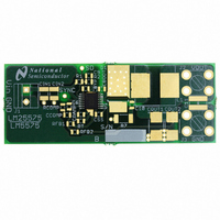
Manufacturer Part Number
LM5575BLDT
Description
WEBENCH BUILD IT BOARD LM5575
Manufacturer
National Semiconductor
Series
WEBENCH®, PowerWise®, SIMPLE SWITCHER®r
Specifications of LM5575BLDT
Main Purpose
DC/DC, Step Down
Outputs And Type
1, Non-Isolated
Voltage - Output
1.23 ~ 70V
Current - Output
1.5A
Voltage - Input
6 ~ 75V
Regulator Topology
Buck
Board Type
Partially Populated - Main IC Only
Utilized Ic / Part
LM5575
Lead Free Status / RoHS Status
Lead free / RoHS Compliant
Power - Output
-
Frequency - Switching
-


www.national.com
The selected operating frequency must be less than Fsw
(max) calculated above, if not reduce the operating frequen-
cy.
Step 4. Calculate the value of Rt for the selected operating
frequency.
Step 5. Calculate the value of L1.
Select the nearest standard inductor value. During an over-
load condition the peak inductor current is limited to 2.1A
nominal (2.5A maximum). The selected inductor must be rat-
ed for peak current of at least 2.5 Amps.
Step 6. Calculate the value of C
Step 7. Set Rfb2 to 5kOhms if Vout[1] is less than or equal to
5 Volts. If Vout[1] is greater than 5V set Rfb2 to 10K Ohms.
Calculate the value of Rfb1:
Step 8. Select the re-circulating diode, D1. A Schottky type
diode is required for all applications. Ultra-fast diodes are not
recommended and may result in damage to the IC due to re-
verse recovery current transients. The reverse breakdown
rating should be greater than the Input Voltage Max Spec[3],
plus some safety margin. For worst case design, assume a
short circuit load condition. In this case the diode will carry the
output current almost continuously. This current can be as
high as 2.5A. Assuming a 0.6V drop across the diode, the
maximum diode power dissipation can be as high as 1.5W.
An SMC or SMB case is recommended.
Selected operating frequency Fsw:
Selected value for R1:
Selected value of L1:
Selected value of C
Selected value of Rfb2:
Selected value of Rfb1:
C
RAMP
RAMP
:
= L1[7] x 10
RAMP
:
-5
Ohms [6]
Henrys [7]
Farads [8]
Ohms [9]
Ohms [10]
Hz [5]
2
Step 9. A good quality input capacitor(s) is necessary to limit
the ripple voltage at the VIN pin while supplying most of the
switch current during the on-time. The minimum RMS ripple
current rating for the input capacitor(s) is 0.75 Amp. A quality
ceramic capacitor with a low ESR is recommended. The input
capacitor voltage rating should be greater than the Input Volt-
age Max Spec [3], plus some safety margin. A guide to select
the input capacitor(s) value in proportion to the operating fre-
quency is:
Step 10. The output capacitor(s) smooth the inductor ripple
current and provide a source of charge for transient loading
conditions. A good starting point for the output capacitance is
to use a ceramic capacitor (10 µF to 100 µF) An additional low
ESR organic or tantalum capacitor (22 µF to 220 µF) could be
added in parallel for applications with large load transients.
The ceramic capacitor provides ultra low ESR to reduce the
output ripple voltage and noise spikes, while the larger bulk
capacitor provides a source of charge for transient loading
conditions. The output capacitor voltage rating should be
greater than the Output Voltage Spec [1], plus some safety
margin. An approximation for the output ripple voltage is:
Step 11. Ccomp and Rcomp configure the error amplifier gain
characteristics to accomplish a stable overall loop gain. One
advantage of current mode control is the ability to close the
loop with only two feedback components. Calculate the value
of Rcomp:
Calculate the value of Ccomp
Step 12. Shown in the following table is the Bill of Materials
for your design. Transcribe each value [#] from worksheet
above into the following table. Congratulations, you’re done.
Selected diode part number:
Selected value for Cin:
Selected value for Cout:
Selected value of Rcomp:
Selected value of Ccomp:
[11]
Farads [12]
Farads [13]
Ohms [14]
Farads [15]
Related parts for LM5575BLDT
Image
Part Number
Description
Manufacturer
Datasheet
Request
R

Part Number:
Description:
National Semiconductor [8-Bit D/A Converter]
Manufacturer:
National Semiconductor
Datasheet:
Part Number:
Description:
National Semiconductor [Media Coprocessor]
Manufacturer:
National Semiconductor
Datasheet:
Part Number:
Description:
Digitally Controlled Tone and Volume Circuit with Stereo Audio Power Amplifier, Microphone Preamp Stage and National 3D Sound
Manufacturer:
National Semiconductor
Datasheet:
Part Number:
Description:
Digitally Controlled Tone and Volume Circuit with Stereo Audio Power Amplifier, Microphone Preamp Stage and National 3D Sound
Manufacturer:
National Semiconductor
Datasheet:
Part Number:
Description:
AC97 Rev 2 Codec with Sample Rate Conversion and National 3D Sound
Manufacturer:
National Semiconductor
Part Number:
Description:
Manufacturer:
National Semiconductor
Datasheet:
Part Number:
Description:
Manufacturer:
National Semiconductor
Datasheet:
Part Number:
Description:
General Purpose, Low Voltage, Low Power, Rail-to-Rail Output Operational Amplifiers
Manufacturer:
National Semiconductor
Datasheet:
Part Number:
Description:
8-bit 20 MSPS flash A/D converter.
Manufacturer:
National Semiconductor
Datasheet:
Part Number:
Description:
Low Noise Quad Operational Amplifier
Manufacturer:
National Semiconductor
Datasheet:
Part Number:
Description:
Quad Differential Line Receivers
Manufacturer:
National Semiconductor
Datasheet:
Part Number:
Description:
Quad High Speed Trapezoidal? Bus Transceiver
Manufacturer:
National Semiconductor
Datasheet:
Part Number:
Description:
Dual Line Receiver
Manufacturer:
National Semiconductor
Datasheet:
Part Number:
Description:
TTL to 10k ECL Level Translator with Latch
Manufacturer:
National Semiconductor
Datasheet: