LM2704EV National Semiconductor, LM2704EV Datasheet - Page 8
LM2704EV
Manufacturer Part Number
LM2704EV
Description
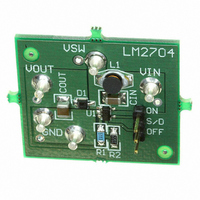
BOARD EVALUATION LM2704
Manufacturer
National Semiconductor
Specifications of LM2704EV
Main Purpose
DC/DC, Step Up
Outputs And Type
1, Non-Isolated
Voltage - Output
20V
Current - Output
550mA
Voltage - Input
2.2 ~ 7V
Regulator Topology
Boost
Board Type
Fully Populated
Utilized Ic / Part
LM2704
Silicon Manufacturer
National
Silicon Core Number
LM2704
Kit Application Type
Power Management - Voltage Regulator
Application Sub Type
Step Up DC/DC Converter
Kit Contents
LM2604 IC Step Up Converter
Rohs Compliant
No
Lead Free Status / RoHS Status
Not applicable / Not applicable
Power - Output
-
Frequency - Switching
-


www.national.com
Operation
The LM2704 features a constant off-time control scheme.
Operation can be best understood by referring to Figure 2
and Figure 3. Transistors Q1 and Q2 and resistors R3 and
R4 of Figure 2 form a bandgap reference used to control the
output voltage. When the voltage at the FB pin is less than
1.237V, the Enable Comp in Figure 2 enables the device and
the NMOS switch is turned on pulling the SW pin to ground.
When the NMOS switch is on, current begins to flow through
inductor L while the load current is supplied by the output
capacitor C
peak current limit, the CL Comp trips and the 400ns One
Shot turns off the NMOS switch. The SW voltage will then
rise to the output voltage plus a diode drop and the inductor
current will begin to decrease as shown in Figure 3. During
this time the energy stored in the inductor is transferred to
C
switch is turned on and energy is stored in the inductor
again. This energy transfer from the inductor to the output
causes a stepping effect in the output ripple as shown in
Figure 3.
This cycle is continued until the voltage at FB reaches
1.237V. When FB reaches this voltage, the enable compara-
tor then disables the device turning off the NMOS switch and
reducing the Iq of the device to 40uA. The load current is
then supplied solely by C
decreasing slope at the output as shown in Figure 3. When
the FB pin drops slightly below 1.237V, the enable compara-
tor enables the device and begins the cycle described pre-
viously. The SHDN pin can be used to turn off the LM2704
and reduce the I
voltage will be a diode drop lower than the input voltage.
Application Information
INDUCTOR SELECTION
The appropriate inductor for a given application is calculated
using the following equation:
where V
current limit found in the Typical Performance Characteris-
tics section, and T
equation be sure to use the minimum input voltage for the
application, such as for battery powered applications. For
the LM2704 constant-off time control scheme, the NMOS
power switch is turned off when the current limit is reached.
There is approximately a 200ns delay from the time the
current limit is reached in the NMOS power switch and when
the internal logic actually turns off the switch. During this
200ns delay, the peak inductor current will increase. This
increase in inductor current demands a larger saturation
current rating for the inductor. This saturation current can be
approximated by the following equation:
Choosing inductors with low ESR decrease power losses
and increase efficiency.
OUT
and the load. After the 400ns off-time the NMOS
D
is the schottky diode voltage, I
OUT
. Once the current in the inductor reaches the
q
OFF
to 0.01µA. In shutdown mode the output
(Continued)
is the switch off time. When using this
OUT
indicated by the gradually
CL
is the switch
8
Care should be taken when choosing an inductor. For appli-
cations that require an input voltage that approaches the
output voltage, such as when converting a Li-Ion battery
voltage to 5V, the 400ns off time may not be enough time to
discharge the energy in the inductor and transfer the energy
to the output capacitor and load. This can cause a ramping
effect in the inductor current waveform and an increased
ripple on the output voltage. Using a smaller inductor will
cause the I
ripple further. This can be solved by adding a 4.7pF capaci-
tor across the R
increasing the output capacitor. A smaller inductor can then
be used to ensure proper discharge in the 400ns off time.
DIODE SELECTION
To maintain high efficiency, the average current rating of the
schottky diode should be larger than the peak inductor cur-
rent, I
switching speeds are ideal for increasing efficiency in por-
table applications. Choose a reverse breakdown of the
schottky diode larger than the output voltage.
CAPACITOR SELECTION
Choose low ESR capacitors for the output to minimize output
voltage ripple. Multilayer ceramic capacitors are the best
choice. For most applications, a 1µF ceramic capacitor is
sufficient. For some applications a reduction in output volt-
age ripple can be achieved by increasing the output capaci-
tor.
Local bypassing for the input is needed on the LM2704.
Multilayer ceramic capacitors are a good choice for this as
well. A 4.7µF capacitor is sufficient for most applications. For
additional bypassing, a 100nF ceramic capacitor can be
used to shunt high frequency ripple on the input.
LAYOUT CONSIDERATIONS
The input bypass capacitor C
be placed close to the IC. This will reduce copper trace
resistance which effects input voltage ripple of the IC. For
additional input voltage filtering, a 100nF bypass capacitor
can be placed in parallel with C
quency noise to ground. The output capacitor, C
also be placed close to the IC. Any copper trace connections
for the Cout capacitor can increase the series resistance,
which directly effects output voltage ripple. The feedback
network, resistors R1 and R2, should be kept close to the FB
pin to minimize copper trace connections that can inject
noise into the system. The ground connection for the feed-
back resistor network should connect directly to an analog
ground plane. The analog ground plane should tie directly to
the GND pin. If no analog ground plane is available, the
ground connection for the feedback network should tie di-
rectly to the GND pin. Trace connections made to the induc-
tor and schottky diode should be minimized to reduce power
dissipation and increase overall efficiency.
PK
. Schottky diodes with a low forward drop and fast
PK
to increase and will increase the output voltage
F1
feedback resistor (Figure 2) and slightly
IN
, as shown in Figure 1, must
IN
to shunt any high fre-
OUT
, should
Related parts for LM2704EV
Image
Part Number
Description
Manufacturer
Datasheet
Request
R

Part Number:
Description:
Micropower Step-up Dc/dc Converter With 550ma Peak Current Limit
Manufacturer:
National Semiconductor Corporation
Datasheet:
Part Number:
Description:
Micropower Step-up DC/DC Converter with 550mA Peak Current Limit
Manufacturer:
NSC [National Semiconductor]
Datasheet:

Part Number:
Description:
National Semiconductor [8-Bit D/A Converter]
Manufacturer:
National Semiconductor
Datasheet:
Part Number:
Description:
National Semiconductor [Media Coprocessor]
Manufacturer:
National Semiconductor
Datasheet:
Part Number:
Description:
Digitally Controlled Tone and Volume Circuit with Stereo Audio Power Amplifier, Microphone Preamp Stage and National 3D Sound
Manufacturer:
National Semiconductor
Datasheet:
Part Number:
Description:
Digitally Controlled Tone and Volume Circuit with Stereo Audio Power Amplifier, Microphone Preamp Stage and National 3D Sound
Manufacturer:
National Semiconductor
Datasheet:
Part Number:
Description:
AC97 Rev 2 Codec with Sample Rate Conversion and National 3D Sound
Manufacturer:
National Semiconductor
Part Number:
Description:
Manufacturer:
National Semiconductor
Datasheet:
Part Number:
Description:
Manufacturer:
National Semiconductor
Datasheet:
Part Number:
Description:
General Purpose, Low Voltage, Low Power, Rail-to-Rail Output Operational Amplifiers
Manufacturer:
National Semiconductor
Datasheet:
Part Number:
Description:
8-bit 20 MSPS flash A/D converter.
Manufacturer:
National Semiconductor
Datasheet:
Part Number:
Description:
Low Noise Quad Operational Amplifier
Manufacturer:
National Semiconductor
Datasheet:
Part Number:
Description:
Quad Differential Line Receivers
Manufacturer:
National Semiconductor
Datasheet:
Part Number:
Description:
Quad High Speed Trapezoidal? Bus Transceiver
Manufacturer:
National Semiconductor
Datasheet: