LM20143EVAL National Semiconductor, LM20143EVAL Datasheet - Page 5
LM20143EVAL
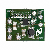
Manufacturer Part Number
LM20143EVAL
Description
BOARD EVAL 3A POWERWISE LM20143
Manufacturer
National Semiconductor
Series
PowerWise®r
Specifications of LM20143EVAL
Main Purpose
DC/DC, Step Down
Outputs And Type
1, Non-Isolated
Voltage - Output
1.2V
Current - Output
3A
Voltage - Input
2.95 ~ 5.5V
Regulator Topology
Buck
Frequency - Switching
1.5MHz
Board Type
Fully Populated
Utilized Ic / Part
LM20143
Lead Free Status / RoHS Status
Not applicable / Not applicable
Power - Output
-


conditions for the device are known, the transient response
can be optimized by reducing the value of C
the value for R
R
Once the value of C
a zero in the control loop to cancel the output filter pole. This
resistor can be sized according to the equation:
For stability purposes the device should be compensated for
the maximum output current expected in the application.
C
A second compensation capacitor C
designs to provide a high frequency pole, useful for cancelling
a possible zero introduced by the ESR of the output capacitor.
For the LM20143 evaluation board, the C
populated, as the low ESR ceramic capacitor used on the
output does not contribute a zero to the control loop before
the crossover frequency. If the ceramic capacitor on the eval-
uation board is replaced with a different capacitor having
significant ESR, the required value of the capacitor C
be estimated by the equation:
C1
C2
C1
as outlined in the next section.
C1
is known, resistor R
C2
can be used in some
C1
C2
C1
is used to place
and calculating
footprint is un-
C2
can
5
R
The value for R
For this evaluation board a value of 49.9 kΩ was chosen
which sets oscillator frequency to 1.5 MHz. The value of R
can be adjusted to support operating frequencies from 500
kHz to 1.5 MHz by using the equation:
Where, f
frequency adjust resistor in kΩ.
R
The resistors labeled R
from V
the voltage regulator. Nominally, the output of the LM20143
evaluation board is set to 1.2V, giving resistor values of
R
is required, the value of R
equation:
R
T
FB1
FB1
FB2
= 4.99 kΩ and R
does not need to be changed from its value of 10 kΩ.
and R
OUT
SW
to the feedback pin that is used to set the output of
FB2
is the switching frequency in kHz, and R
T
will set the operating frequency of the device.
FB2
FB1
= 10 kΩ. If a different output voltage
FB1
and R
can be adjusted according to the
FB2
create a voltage divider
www.national.com
T
is the
T
Related parts for LM20143EVAL
Image
Part Number
Description
Manufacturer
Datasheet
Request
R

Part Number:
Description:
MODULE TXRX BLUETOOTH 2 18SMD
Manufacturer:
Flexipanel
Datasheet:

Part Number:
Description:
MODULE TXRX BLUETOOTH 2 18DIP
Manufacturer:
Flexipanel
Datasheet:

Part Number:
Description:
LM20 2.4V, 10?A, SC70, micro SMD Temperature Sensor
Manufacturer:
National Semiconductor
Datasheet:
Part Number:
Description:
National Semiconductor [8-Bit D/A Converter]
Manufacturer:
National Semiconductor
Datasheet:
Part Number:
Description:
National Semiconductor [Media Coprocessor]
Manufacturer:
National Semiconductor
Datasheet:
Part Number:
Description:
Digitally Controlled Tone and Volume Circuit with Stereo Audio Power Amplifier, Microphone Preamp Stage and National 3D Sound
Manufacturer:
National Semiconductor
Datasheet:
Part Number:
Description:
Digitally Controlled Tone and Volume Circuit with Stereo Audio Power Amplifier, Microphone Preamp Stage and National 3D Sound
Manufacturer:
National Semiconductor
Datasheet:
Part Number:
Description:
AC97 Rev 2 Codec with Sample Rate Conversion and National 3D Sound
Manufacturer:
National Semiconductor
Part Number:
Description:
Manufacturer:
National Semiconductor
Datasheet:
Part Number:
Description:
Manufacturer:
National Semiconductor
Datasheet:
Part Number:
Description:
General Purpose, Low Voltage, Low Power, Rail-to-Rail Output Operational Amplifiers
Manufacturer:
National Semiconductor
Datasheet:
Part Number:
Description:
8-bit 20 MSPS flash A/D converter.
Manufacturer:
National Semiconductor
Datasheet:
Part Number:
Description:
Low Noise Quad Operational Amplifier
Manufacturer:
National Semiconductor
Datasheet:
Part Number:
Description:
Quad Differential Line Receivers
Manufacturer:
National Semiconductor
Datasheet: