DK86064-2 Fujitsu Semiconductor America Inc, DK86064-2 Datasheet
DK86064-2
Specifications of DK86064-2


Related parts for DK86064-2


DK86064-2 Summary of contents
Page 1
Datasheet MB86064 Dual 14-bit 1GSa/s DAC The Fujitsu MB86064 is a Dual 14-bit 1GSa/s digital to analog converter (DAC), delivering exceptional dynamic performance. Each high performance DAC core is capable of generating multi-standard, multi-carrier communication transmit signals, suitable for 2, ...
Page 2
Contents 1 Functional Description . . . . . . . . . . . . . . . . . . . . . . . . . . . . . . . . . . . . ...
Page 3
October 2005 Version 1.2 FME/MS/DAC80/DS/4972 MB86064 Dual 14-bit 1GSa/s DAC 5.4 Ordering Information . . . . . . . . . . . . . . . . . . . . . . . . . . . ...
Page 4
Functional Description The MB86064 is a high performance Dual 14-bit 1GSa/s DAC. In addition to two DAC cores the device features a host of features designed to help both system integration and operation. A functional block diagram is shown ...
Page 5
October 2005 Version 1.2 FME/MS/DAC80/DS/4972 MB86064 Dual 14-bit 1GSa/s DAC 1.1 Clock The device requires an input clock at half the DAC conversion rate, with sufficient spectral purity to not impact the target analog output performance. The DAC cores are ...
Page 6
The delay settings are programmed through register DAC CORE CLOCK DELAYS, bits dac_clk_dly and dac_latch_dly. Based on detailed evaluation by Fujitsu these registers should be programmed in accordance with the recommendations given in Table 1. Table 1: DAC Core ...
Page 7
October 2005 Version 1.2 FME/MS/DAC80/DS/4972 MB86064 Dual 14-bit 1GSa/s DAC 1.1.4 Clock Outputs Two clock outputs, CLK1_OUT and CLK2_OUT, are provided to enable synchronisation of data generating devices to the DAC. The reference clock used by the Clock Output block ...
Page 8
Table 6: DAC Core Register: SYSTEM CLOCK DELAYS [0x1C1] (Part Label 3 0 clkout2_clk_dly : 1 The clock outputs are designed to drive a doubly-terminated LVDS line (7mA drive into a bridged 50 load) for the best ...
Page 9
October 2005 Version 1.2 FME/MS/DAC80/DS/4972 MB86064 Dual 14-bit 1GSa/s DAC generating device, can be incorporated in the feedback loop of a Delay-Locked Loop (DLL) or Phase- Locked Loop (PLL) clock generator, within the generating device. This enables the system to ...
Page 10
This example used an Altera Stratix FPGA evaluation platform driving a Fujitsu development kit at 800MSa/s. Another circuit implementation would exhibit different absolute timings but similar relative adjustments. Having evaluated a prototype design and final loop clock delay settings chosen, ...
Page 11
October 2005 Version 1.2 FME/MS/DAC80/DS/4972 MB86064 Dual 14-bit 1GSa/s DAC 1.2 DAC Data Each DAC core can be considered as two identical halves, referred to as ODD and EVEN. EVEN samples are latched on the falling edge of Clock Output, ...
Page 12
Table 9: Waveform Memory Module Register: WMM CONFIG [0x00] (Part WMM CONFIG Label (bit) 4 data_direct Port A data input 14-bit LVDS Port B data input 14-bit LVDS Figure 7 Direct Data Routing from the LVDS Interface ...
Page 13
October 2005 Version 1.2 FME/MS/DAC80/DS/4972 MB86064 Dual 14-bit 1GSa/s DAC When using the Loop Clock, the delay set by loop_clk_dly (Table 7) opposes this and effectively advances the input data relative to the reference clock edge. Together these adjustments provide ...
Page 14
Table 10: DAC Core Register: DAC CONFIG [0x1C0] DAC CONFIG (bits The appropriate setting of these bits is dependent on the power-down status of the DAC cores, determined by register ...
Page 15
October 2005 Version 1.2 FME/MS/DAC80/DS/4972 MB86064 Dual 14-bit 1GSa/s DAC Analog output performance benefits from the chosen DAC core architecture, identified in Section 1 as similar to two interleaved DACs running at half rate. The big advantage of this approach ...
Page 16
Reset and Power Down Pin X_RESET is the device reset pin. On the falling edge of X_RESET the device is reset and all registers are set to their default values. After a reset most parts of the device are ...
Page 17
October 2005 Version 1.2 FME/MS/DAC80/DS/4972 MB86064 Dual 14-bit 1GSa/s DAC 2 Serial Control Interface A simple 4-wire serial control interface is used to control the MB86064. The serial interface uses pins SERIAL_IN, SERIAL_OUT, SERIAL_CLK and SERIAL_EN. Programmed settings are stored ...
Page 18
SERIAL_CLK SERIAL_IN msb Address Example of zero-filling a register SERIAL_EN SERIAL_OUT Figure 10 Serial Control Interface ‘Write’ Operation SERIAL_CLK SERIAL_IN Address msb SERIAL_EN SERIAL_OUT Figure 11 Serial Control Interface ‘Read’ Operation Production Page Disclaimer : The contents ...
Page 19
October 2005 Version 1.2 FME/MS/DAC80/DS/4972 MB86064 Dual 14-bit 1GSa/s DAC SERIAL_CLK SERIAL_IN & SERIAL_EN SERIAL_OUT Figure 12 Serial Control Interface Timing Requirements For initial testing & evaluation it is assumed that customers will use the Fujitsu PC USB Programming cable ...
Page 20
Waveform Memory Module Enabling the Waveform Memory Module allows interleaving of the LVDS data to drive a single DAC core as well as access to any downloaded waveforms. The on-chip waveform memories allow the DAC cores to be exercised ...
Page 21
October 2005 Version 1.2 FME/MS/DAC80/DS/4972 MB86064 Dual 14-bit 1GSa/s DAC The data multiplexers are controlled by the WMM Registers, WMM [EVEN/ODD] MUX CTRL. Setting of these registers is referred to in the following two sections. Table 12: Waveform Memory Module ...
Page 22
Dual Port, Interleaved LVDS Data via the WMM By routing the external LVDS data through the Waveform Memory Module it is possible to interleave A and B data into one of the DAC cores. To configure the device in ...
Page 23
October 2005 Version 1.2 FME/MS/DAC80/DS/4972 MB86064 Dual 14-bit 1GSa/s DAC 3.2 Waveform Memory Module Operation To make full use of the Waveform Memory Module user waveforms may be downloaded to the on- chip memories. Different waveforms of equal length may ...
Page 24
ODD and EVEN RAM elements within the module allow data to be routed to the ODD and EVEN phase DAC core data latches, similar to when data is input via the LVDS data interface and double edge clocking is used. ...
Page 25
October 2005 Version 1.2 FME/MS/DAC80/DS/4972 MB86064 Dual 14-bit 1GSa/s DAC The WMM [EVEN/ODD] RAM CTRL registers prog_addr fields are used to define the start address of the waveform. These fields should be set order to store a ...
Page 26
Register bit prog_start is used to indicate the start of a write cycle to the RAMs. This bit is self clearing. See section 3.2.2 for details of the write cycle. 3.2.2 Writing Data into the Memories The process of writing ...
Page 27
October 2005 Version 1.2 FME/MS/DAC80/DS/4972 MB86064 Dual 14-bit 1GSa/s DAC Once the RAM Access Controller returns to the idle state, after a successful write sequence, data transfer starts automatically. However, until the other RAM element is programmed and the RAMs ...
Page 28
Electrical Characteristics 4.1 Absolute Maximum Ratings Parameter Supply voltage Analog supply Digital Supply Input Voltage LVDS inputs Digital control inputs Analog Output Voltage Analog Output Current Storage Temperature Junction Temperature T (min (max), AVD33 = +3.3V, AVSS ...
Page 29
October 2005 Version 1.2 FME/MS/DAC80/DS/4972 MB86064 Dual 14-bit 1GSa/s DAC 4.3 DC Specifications Parameter DC Accuracy Integral Non Linearity Differential Non Linearity Analog output Full scale signal output current Current at each output Load resistance (single ended) Output resistance Output ...
Page 30
AC Specifications Parameter Spurious-Free Dynamic Range Single tone at -1dBFS, 800MSa/ 400MHz 20 MHz 40 MHz 70 MHz 140 MHz 300 MHz Single tone at -1dBFS, 1GSa/ 500MHz 20 MHz 40 MHz 70 MHz 140 ...
Page 31
October 2005 Version 1.2 FME/MS/DAC80/DS/4972 MB86064 Dual 14-bit 1GSa/s DAC Parameter (Continued) Adjacent Channel Leakage Ratio 1 x UMTS carrier, 5MHz channel spacing 30.72MHz centre frequency, 245.76MSa/s 276.48MHz centre frequency, 737.28MSa UMTS carriers, 5MHz channel spacing 276.48MHz centre ...
Page 32
Clock Specifications Parameter Clock Input Maximum clock frequency Square Wave Low time High time Slew rate for minimum wide-band jitter Clock input duty cycle Low-level input voltage High-level input voltage Sinusoidal (recommended) Common mode input voltage Signal level (f ...
Page 33
October 2005 Version 1.2 FME/MS/DAC80/DS/4972 MB86064 Dual 14-bit 1GSa/s DAC 4.7 Serial Interface Timing Specifications Parameter Serial Clock Frequency Serial Clock Mark or Space Setup , SERIAL_IN to SERIAL_CLK rising edge Hold , SERIAL_IN from SERIAL_CLK rising edge Delay , ...
Page 34
Production Page Disclaimer : The contents of this document are subject to change without notice. Customers are advised ...
Page 35
October 2005 Version 1.2 FME/MS/DAC80/DS/4972 MB86064 Dual 14-bit 1GSa/s DAC 5 Mechanical Data 5.1 Pin Assignment X_A10 X_A9 W23 W21 V22 A10 A9 V20 U23 DVSS DVDD U21 T20 X_A8 T22 X_A7 A8 A7 R23 R21 P22 P20 X_A6 X_A5 ...
Page 36
Pin Definition Analog and Clock Interface Pin Nos. Pin Name D10, D14 AVD33 B16, A17 AVD18_A A7, B8 AVD18_B D12 AVD18_CLK C7, B12, C17 AVSS C15 IOUT_A D16 IOUTB_A C9 IOUT_B D8 IOUTB_B C11 BGAP B10 VREF A11 RREF ...
Page 37
October 2005 Version 1.2 FME/MS/DAC80/DS/4972 MB86064 Dual 14-bit 1GSa/s DAC Digital Data Interface Pin Nos. Pin Name F2, F22, G1, M2, U1, DVDD AC7, AB12, AC17, U23, M22, G23 E1, E23, G3, M4, U3, DVSS AA7, Y12, AA17, U21, M20, ...
Page 38
Pin Nos. Pin Name L1 X_B4 X_B5 X_B6 X_B7 X_B8 X_B9 V4 B10 W3 X_B10 AA5 B11 Y6 X_B11 AC5 B12 AB6 X_B12 Y8 B13 ...
Page 39
October 2005 Version 1.2 FME/MS/DAC80/DS/4972 MB86064 Dual 14-bit 1GSa/s DAC 5.3 Package Data Dimensions in millimetres. Ball array viewed from below . Important: This device requires pre-baking at 125°C (257°F) for 24 hours before mounting unless removed from approved vacuum ...
Page 40
Application Notes 6.1 PCB Power & Ground Plane Splits and Decoupling The following guidelines are suggestions to help obtain best performance from the MB86064. The information may be subject to change. The ground plane should not be split into ...
Page 41
October 2005 Version 1.2 FME/MS/DAC80/DS/4972 MB86064 Dual 14-bit 1GSa/s DAC IOUT termination resistors Pin 1 A: Top layer Pin 1 C: Internal layer 1 - IOUTB tracks (thick the termination resistors and CLKINB track (thin) Figure 19 Recommended ...
Page 42
Input Clock Interfacing The differential clock input to the device needs to be biased about the specified typical common mode input voltage. The exact interface circuitry will depend on the functionality required but an example is illustrated in Figure ...
Page 43
October 2005 Version 1.2 FME/MS/DAC80/DS/4972 MB86064 Dual 14-bit 1GSa/s DAC 6.3 Clock Duty Cycle Optimisation Earlier sections of this data sheet document that the DAC core is clocked on both rising and falling edges of the input clock, and that ...
Page 44
Analog Output Interfacing 6.4.1 Transformer Coupled Output Circuit The recommended analog output circuit is a two stage transformer circuit that provides both isolation from the analog ground plane and excellent common-mode rejection, whilst providing the required differential to single-ended ...
Page 45
October 2005 Version 1.2 FME/MS/DAC80/DS/4972 MB86064 Dual 14-bit 1GSa/s DAC necessary, the ground planes that the signals use as a reference plane must be linked together with vias next to the signal vias so that the return currents in the ...
Page 46
Example Setup Register Settings The following sections provide examples of typical configurations for the MB86064 and required register settings. In all cases other registers are assumed their default values, following a device reset. 6.5.1 Dual DAC, ...
Page 47
October 2005 Version 1.2 FME/MS/DAC80/DS/4972 MB86064 Dual 14-bit 1GSa/s DAC • {load waveform data into memories, start addr=0 length=2047(0x7FF)} • {this length corresponds to a vector length of 16k points} • 0x13 0xXXXXXXX • 0x12 0x27FF800 • 0x13 0xXXXXXXX • ...
Page 48
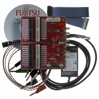
... Development Kit A development kit, reference DK86064-2, is available for the MB86064 Dual 14-bit 1GSa/s DAC. This comprises an evaluation board for the MB86064 and a PC programming cable with associated software. Connections for all analog signals are via SMA connectors, allowing instruments to be connected using standard cables. All digital I/O signals are routed to four 2-row 0.1” headers, allowing the board to be connected to a suitably designed customer’ ...
Page 49
October 2005 Version 1.2 FME/MS/DAC80/DS/4972 MB86064 Dual 14-bit 1GSa/s DAC 7.1 Using DKUSB-1 in Target Applications It is expected that customers can benefit from using Fujitsu’s PC USB Programming cable and accompanying PC software, DKUSB-1, for debug of prototype target ...
Page 50
Appendix A Default Register Settings Appendix A.1 DAC Core Registers Register Address DAC A 190 16 THOLD 01 1001 0000 DAC A 191 16 SEED 01 1001 0001 ...
Page 51
October 2005 Version 1.2 FME/MS/DAC80/DS/4972 MB86064 Dual 14-bit 1GSa/s DAC Appendix A.2 Waveform Memory Module Registers Register Address WMM 00 16 CONFIG 000 0000 WMM EVEN 10 16 CONFIG 001 0000 WMM EVEN 11 16 MUX CTRL 001 0001 WMM ...
Page 52
Worldwide Headquarters Japan Tel: +81 44 754 3753 Fujitsu Limited Fax: +81 44 754 3329 Kamikodanaka 4-1-1 Nakahara-ku Kawasaki-shi Kanagawa-ken 211-8588 Japan http://www.fujitsu.com USA Tel: +1 408 737 5600 Fujitsu Microelectronics America, Inc. Fax: +1 408 737 5999 1250 E. ...