DK86064-2 Fujitsu Semiconductor America Inc, DK86064-2 Datasheet - Page 5
DK86064-2
Manufacturer Part Number
DK86064-2
Description
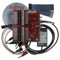
KIT DEB DUAL 14BIT DAC MB86064
Manufacturer
Fujitsu Semiconductor America Inc
Specifications of DK86064-2
Number Of Dac's
2
Number Of Bits
14
Outputs And Type
1, Differential
Sampling Rate (per Second)
1G
Data Interface
Serial
Dac Type
Current
Voltage Supply Source
Analog and Digital
Operating Temperature
-40°C ~ 85°C
Utilized Ic / Part
MB86064
For Use With
865-1111 - DAC DK FPGA ADAPTER BOARD865-1012 - KIT DEV DUAL 14BIT MB86064 SMA
Lead Free Status / RoHS Status
Lead free / RoHS Compliant
Other names
865-1010


October 2005 Version 1.2
FME/MS/DAC80/DS/4972
MB86064 Dual 14-bit 1GSa/s DAC
1.1
The device requires an input clock at half the DAC conversion rate, with sufficient spectral purity to
not impact the target analog output performance. The DAC cores are clocked on both rising and
falling edges of the input clock. This forms an effect of two interleaved converters in each DAC core.
A characteristic of this architecture is a suppressed image of the generated signal, appearing
reflected about Fs(dac)/4 = (Fclk-Fsig). Any duty cycle error in the input clock will exacerbate this
image. This can be minimised by trimming the differential DC offset at the clock input pins.
1.1.1 Input Clock
The input clock should be applied to the MB86064 through input pins CLKIN and CLKINB. The device
is designed to accept a differential sinusoidal clock. Once on chip and converted to CMOS the clock
is distributed to a number of blocks throughout the device. The DAC cores are supplied directly from
the input clock buffer to ensure minimal degradation to the clock’s purity.
1.1.2 DAC Core Clocks Programmable Delays
The DAC core clocks contain programmable delays. These allow adjustment to the point at which
data is clocked into the DAC core and when the analog portion of the DAC subsequently latches the
Copyright © 2004-2005 Fujitsu Microelectronics Europe GmbH
Disclaimer : The contents of this document are subject to change without notice. Customers are advised to consult with FUJITSU sales representatives before
Loop clock output
Loop clock input
Clock input
X_RESET
Clock
ordering.The information and circuit diagrams in this document are presented “as is”, no license is granted by implication or otherwise.
wmm_clk_dly
en_wmm_clk
LVDS
LVDS
0x1C4 – pg21
0x1C1 - pg6
RF
loop_clk_dly
0x1C1 - pg9
Waveform Memory Module
en_ref_clk
0x1C4 - pg7
en_int_term
en_int_term
0x1C4 - pg11
0x1C4 - pg11
Clock to
Figure 2 Clock Distribution
dac_clk_dly
Waveform Memory Module
0x1B2 - pg6
clkout1_cfg
clkout2_cfg
÷ 2
0x00 - pg7
0x00 - pg7
÷ 4
÷ N
÷ 8
Production
DAC cores
Clocks to
dac_latch_dly
0x1B2 - pg6
clkout1_clk_dly
pdn_outcks
clkout2_clk_dly
0x1C3 - pg16
0x1C1 - pg7
0x1C1 - pg8
en_int_term
0x1C4 - pg11
Clock output 1
LVDS
Clock output 2
LVDS
Page 5 of 52
Related parts for DK86064-2
Image
Part Number
Description
Manufacturer
Datasheet
Request
R

Part Number:
Description:
IC POWER SUPPLY MONITOR 8SOP
Manufacturer:
Fujitsu Semiconductor America Inc
Datasheet:
Part Number:
Description:
IC POWER SUPPLY MONITOR 8SOP
Manufacturer:
Fujitsu Semiconductor America Inc
Datasheet:

Part Number:
Description:
IC MCU 60K FLASH 2KB RAM 52LQFP
Manufacturer:
Fujitsu Semiconductor America Inc
Datasheet:

Part Number:
Description:
IC MCU 32BIT 256KB FLASH 120LQFP
Manufacturer:
Fujitsu Semiconductor America Inc
Datasheet:
Part Number:
Description:
IC CTLR TOUCH SENSOR 12CH 30SSOP
Manufacturer:
Fujitsu Semiconductor America Inc
Datasheet:

Part Number:
Description:
IC CTLR TOUCH SENSOR 12CH 40QFN
Manufacturer:
Fujitsu Semiconductor America Inc
Datasheet:
Part Number:
Description:
SYNTHESIZER PLL DUAL INP 20SSOP
Manufacturer:
Fujitsu Semiconductor America Inc
Datasheet:

Part Number:
Description:
SYNTHESZR PLL 1.1GHZ DUAL 16SSOP
Manufacturer:
Fujitsu Semiconductor America Inc
Datasheet:

Part Number:
Description:
IC SSCG EMI RED 8-SOIC
Manufacturer:
Fujitsu Semiconductor America Inc
Datasheet:

Part Number:
Description:
IC SSCG EMI RED 8-TSSOP
Manufacturer:
Fujitsu Semiconductor America Inc
Datasheet:

Part Number:
Description:
IC SSCG EMI RED 8-SOP
Manufacturer:
Fujitsu Semiconductor America Inc
Datasheet:

Part Number:
Description:
SYNTHESIZER PLL 2.5GHZ 16SSOP
Manufacturer:
Fujitsu Semiconductor America Inc
Datasheet:
Part Number:
Description:
SYNTHESIZER PLL 1.2GHZ 16SSOP
Manufacturer:
Fujitsu Semiconductor America Inc
Datasheet:

Part Number:
Description:
SYNTHESIZER PLL 2.5GHZ 16BCC
Manufacturer:
Fujitsu Semiconductor America Inc
Datasheet:

Part Number:
Description:
IC SSCG EMI RED 8-SOP
Manufacturer:
Fujitsu Semiconductor America Inc
Datasheet: