EVAL-AD5379EBZ Analog Devices Inc, EVAL-AD5379EBZ Datasheet - Page 22
EVAL-AD5379EBZ
Manufacturer Part Number
EVAL-AD5379EBZ
Description
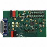
BOARD EVALUATION FOR AD5379
Manufacturer
Analog Devices Inc
Datasheet
1.AD5379ABCZ.pdf
(28 pages)
Specifications of EVAL-AD5379EBZ
Number Of Dac's
40
Number Of Bits
14
Outputs And Type
40, Single Ended
Sampling Rate (per Second)
50k
Data Interface
Serial, Parallel
Settling Time
20µs
Dac Type
Voltage
Voltage Supply Source
Analog and Digital, Dual ±
Operating Temperature
-40°C ~ 85°C
Utilized Ic / Part
AD5379
Lead Free Status / RoHS Status
Lead free / RoHS Compliant


AD5379
INTERFACES
The AD5379 contains a serial and a parallel interface. The
active interface is selected via the SER/ PAR pin.
The AD5379 uses an internal FIFO memory to allow high
speed successive writes in both serial and parallel modes. The
user can continue writing new data to the AD5379 while write
instructions are being executed. The BUSY signal goes low while
instructions in the FIFO are being executed. Up to 120 successive
instructions can be written to the FIFO at maximum speed.
When the FIFO is full, additional writes to the AD5379 are
ignored.
To minimize both the power consumption of the device and
on-chip digital noise, the active interface powers up fully only
when the device is being written to, that is, on the falling edge
of WR or on the falling edge of SYNC .
All digital interfaces are 2.5 V LVTTL-compatible when
operating from a 2.7 V to 3.6 V V
PARALLEL INTERFACE
A pull-down on the SER/ PAR pin makes the parallel interface
the default. If using the parallel interface, the SER/ PAR pin can
be left unconnected.
parallel write to the AD5379. The parallel interface is controlled
by the following pins.
CS Pin
Active low device select pin.
WR Pin
On the rising edge of WR , with CS low, the address values at
Pin A7 to Pin A0 are latched, and data values at Pin DB13 to
Pin DB0 are loaded into the selected AD5379 input registers.
REG1, REG0 Pins
The REG1 and REG0 pins determine the destination register of
the data being written to the AD5379. See Table 11.
Table 11. Register Selection
REG1
1
1
0
0
DB13 to DB0 Pins
The AD5379 accepts a straight, 14-bit parallel word on Pin DB0
to Pin DB13, where Pin DB13 is the MSB and Pin DB0 is the
LSB. See Table 12, Table 13, Table 14, Table 15, and Table 16.
REG0
1
0
1
0
Figure 6
Register Selected
Input data register (x1)
Offset register (c)
Gain register (m)
Special function register
shows the timing diagram for a
CC
supply.
Rev. B | Page 22 of 28
A7 to A0 Pins
Each of the 40 DAC channels can be individually addressed. In
addition, several channel groupings enable the user to simulta-
neously write the same data to multiple DAC channels. Address
Bits A7 to A4 are decoded to select one group or multiple
groups of registers. Address Bits A3 to A0 select one of ten
input data registers (x1), offset registers (c), or gain registers
(m). See Table 17.
SERIAL INTERFACE
The SER/ PAR pin must be tied high to enable the serial inter-
face and disable the parallel interface. The serial interface is
controlled by five pins, as follows.
SYNC , DIN, SCLK
Standard 3-wire interface pins.
DCEN
Selects standalone mode or daisy-chain mode.
SDO
Data out pin for daisy-chain mode.
Figure 4 and Figure 5 show the timing diagrams for a serial
write to the AD5379 in standalone and daisy-chain modes,
respectively.
The 24-bit data word format for the serial interface is shown in
Figure 21.
Standalone Mode
By connecting the DCEN (daisy-chain enable) pin low,
standalone mode is enabled. The serial interface works with
both a continuous and a burst serial clock. The first falling edge
of SYNC starts the write cycle and resets a counter that counts
the number of serial clocks to ensure that the correct number of
bits is shifted into the serial shift register. Additional edges on
SYNC are ignored until 24 bits are shifted into the register.
Once 24 bits are shifted into the serial shift register, the SCLK is
ignored. In order for another serial transfer to take place, the
counter must be reset by the falling edge of SYNC .
MSB
GROUP/CHANNEL
SELECT BITS
A7–A0
REGISTER SELECT
BITS
REG1
Figure 21. Serial Data Format
REG0
REGISTER DATA BITS
DB13–DB0
LSB
Related parts for EVAL-AD5379EBZ
Image
Part Number
Description
Manufacturer
Datasheet
Request
R


Part Number:
Description:
BOARD EVAL FOR SI270X-A
Manufacturer:
Silicon Laboratories Inc
Datasheet:

Part Number:
Description:
BUCK CONV REF DESIGN KIT IP1201
Manufacturer:
International Rectifier
Datasheet:
Part Number:
Description:
BOARD DEMO SYNC DUAL BUCK CNVTER
Manufacturer:
International Rectifier
Datasheet:
Part Number:
Description:
BOARD DEMO SYNC BUCK CONVETER
Manufacturer:
International Rectifier
Datasheet:

Part Number:
Description:
EVALBOARD/EB Omnidirectional microphone - Analog
Manufacturer:
Analog Devices
Datasheet:
Part Number:
Description:
EVALBOARD/EB Omnidirectional microphone - Analog
Manufacturer:
Analog Devices
Datasheet:


Part Number:
Description:
BOARD EVAL LED DRIVER LT3756
Manufacturer:
Linear Technology
Datasheet:

Part Number:
Description:
BOARD EVAL FOR AD7741/7742
Manufacturer:
Analog Devices Inc
Datasheet:

Part Number:
Description:
±1.7g Dual-Axis IMEMS Accelerometer Evaluation Board
Manufacturer:
Analog Devices Inc
Datasheet:

Part Number:
Description:
IC MULTIPLIER ANALOG 8-SOIC T/R
Manufacturer:
Analog Devices Inc
Datasheet:

Part Number:
Description:
IC ANALOG MULTIPLIER 8-DIP
Manufacturer:
Analog Devices Inc
Datasheet:
Part Number:
Description:
IC ANALOG MULTIPLIER 8-SOIC
Manufacturer:
Analog Devices Inc
Datasheet:
Part Number:
Description:
IC ANALOG MULTIPLIER 8-DIP
Manufacturer:
Analog Devices Inc
Datasheet: