LM2796TLEV National Semiconductor, LM2796TLEV Datasheet - Page 3
LM2796TLEV
Manufacturer Part Number
LM2796TLEV
Description
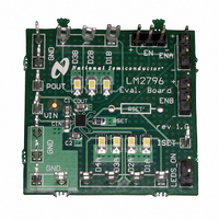
BOARD EVALUATION LM2796TL
Manufacturer
National Semiconductor
Series
PowerWise®r
Specifications of LM2796TLEV
Current - Output / Channel
20mA
Outputs And Type
7, Non-Isolated
Voltage - Output
4 V
Features
Charge Pump
Voltage - Input
2.7 ~ 5.5V
Utilized Ic / Part
LM2796
Lead Free Status / RoHS Status
Not applicable / Not applicable


I
I
I
I
V
I
R
V
Dxx
Dxx-MATCH
Q
SD
Dxx
Symbol
SET
HR
OUT
Absolute Maximum Ratings
If Military/Aerospace specified devices are required,
please contact the National Semiconductor Sales Office/
Distributors for availability and specifications.
Electrical Characteristics
Limits in standard typeface and typical values apply for T
temperature range (-30˚C ≤ T
Group B LEDs not ON simultaneously (ENA = V
C
V
EN, ENA, ENB pin voltages
Continuous Power Dissipation
(Note 3)
Junction Temperature (T
Storage Temperature Range
Maximum Lead Temperature
(Soldering, 10 sec.)
ESD Rating (Note 4)Human Body
Model:
Machine Model
/I
2
IN
, and C
SET
pin voltage
Output Current Regulation
Current Matching Between Any
Two Group A Outputs or Group
B Outputs
Quiescent Supply Current
Shutdown Supply Current
I
Output Current to Current Set
Ratio
Charge Pump Output Resistance
(Note 11)
Current Source Headroom
Voltage Requirement (Note 12)
POUT
SET
Pin Voltage
= 1µF. (Note 8)
Parameter
J-MAX
J
)
≤ +85˚C) . Unless otherwise specified: V
-0.3V to (V
-65
Internally Limited
(Notes 2, 7)
3.0V ≤ V
2.5V ≤ V
R
3.0V ≤ V
2.5V ≤ V
R
3.0V ≤ V
2.5V ≤ V
R
2.7V ≤ V
2.5V ≤ V
R
ENA and ENB ON (all 7 I
V
V
2.7V ≤ V
No Load Current,
EN = ON, ENA = ENB = OFF
2.7V ≤ V
2.7V ≤ V
V
I
R
(I
I
R
(I
o
Dxx
Dxx
-0.3V to 7.1V
C to +150
Dxx
Dxx
SET
SET
SET
SET
IN
IN
IN
SET
SET
w/ 5.6V max
(Notes 1, 2)
= 3.0V, C
= 3.0V (Note 10)
= 3.0V
IN
= 95% X I
= 95%X I
(nom) ≈ 15mA)
(nom) ≈ 10mA)
= 8.35kΩ
= 6.25kΩ
= 12.5kΩ
= 8.35kΩ
= 8.35kΩ
= 12.5kΩ
IN
and ENB = GND, or ENA = GND and ENB = V
+0.3V)
150
265
2.0kV
IN
Dxx
IN
Dxx
IN
Dxx
IN
Dxx
IN
IN
IN
200V
o
≤ 4.2V, and V
≤ 5.5V;
≤ 5.5V;
≤ 3.0V;
≤ 4.2V;
≤ 5.5V, EN = OFF
≤ 5.5V
o
o
≤ 3.8V;
≤ 3.6V;
≤ 3.9V;
≤ 3.3V;
C
C
C
J
IN
Dxx
Dxx
= 25
= C
(nom)
(nom)
Condition
3
o
OUT
C. Limits in boldface type apply over the full operating junction
Operating Rating
Thermal Properties
Input Voltage Range
Junction Temperature (T
Ambient Temperature (T
(Note 5)
Juntion-to-Ambient Thermal
Resistance (θ
= 2.2µF
IN
DX
IN
= 5.5V
outputs active),
= 3.6V; V
JA
), (Note 6)
Dxx
= 3.6V; V(EN) = 2.0V; Group A and
A
J
) Range
) Range
(-8%)
13.8
Min
(Notes 1, 2)
IN
); R
SET
1.25
Typ
100
320
220
3.5
2.7
15
20
10
15
15
1
3
= 8.35kΩ; C
-30˚C to +125˚C
-30˚C to +85˚C
(+8%)
2.7V to 5.5V
Max
16.2
4.5
6
www.national.com
100˚C/W
IN
, C
Units
(%)
mA
mA
mA
mA
mA
mA
mV
µA
%
Ω
V
1
,
Related parts for LM2796TLEV
Image
Part Number
Description
Manufacturer
Datasheet
Request
R

Part Number:
Description:
Accurate, 120 C-150 C Factory Preset Thermostat Lm27 Form
Manufacturer:
National Semiconductor Corporation
Datasheet:

Part Number:
Description:
Factory Preset Thermostat
Manufacturer:
National Semiconductor
Datasheet:
Part Number:
Description:
National Semiconductor [8-Bit D/A Converter]
Manufacturer:
National Semiconductor
Datasheet:
Part Number:
Description:
National Semiconductor [Media Coprocessor]
Manufacturer:
National Semiconductor
Datasheet:
Part Number:
Description:
Digitally Controlled Tone and Volume Circuit with Stereo Audio Power Amplifier, Microphone Preamp Stage and National 3D Sound
Manufacturer:
National Semiconductor
Datasheet:
Part Number:
Description:
Digitally Controlled Tone and Volume Circuit with Stereo Audio Power Amplifier, Microphone Preamp Stage and National 3D Sound
Manufacturer:
National Semiconductor
Datasheet:
Part Number:
Description:
AC97 Rev 2 Codec with Sample Rate Conversion and National 3D Sound
Manufacturer:
National Semiconductor
Part Number:
Description:
Manufacturer:
National Semiconductor
Datasheet:
Part Number:
Description:
Manufacturer:
National Semiconductor
Datasheet:
Part Number:
Description:
General Purpose, Low Voltage, Low Power, Rail-to-Rail Output Operational Amplifiers
Manufacturer:
National Semiconductor
Datasheet:
Part Number:
Description:
8-bit 20 MSPS flash A/D converter.
Manufacturer:
National Semiconductor
Datasheet:
Part Number:
Description:
Low Noise Quad Operational Amplifier
Manufacturer:
National Semiconductor
Datasheet:
Part Number:
Description:
Quad Differential Line Receivers
Manufacturer:
National Semiconductor
Datasheet:
Part Number:
Description:
Quad High Speed Trapezoidal? Bus Transceiver
Manufacturer:
National Semiconductor
Datasheet: