LP5526TLEV National Semiconductor, LP5526TLEV Datasheet - Page 24
LP5526TLEV
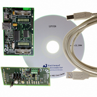
Manufacturer Part Number
LP5526TLEV
Description
BOARD EVAL LP5526 LMU LED DRIVER
Manufacturer
National Semiconductor
Series
PowerWise®r
Specifications of LP5526TLEV
Current - Output / Channel
150mA
Outputs And Type
2 (25mA), 1 (150mA)
Voltage - Output
20 V
Features
Camera Flash, Dimmable, RGB Controller
Voltage - Input
3 ~ 5.5V
Utilized Ic / Part
LP5526
Lead Free Status / RoHS Status
Not applicable / Not applicable


www.national.com
Recommended External Components
OUTPUT CAPACITOR, C
The output capacitor C
the output ripple voltage. In general, the higher the value of
C
ramic capacitors with low ESR are the best choice. At the
lighter loads, the low ESR ceramics offer a much lower
V
At the higher loads, the ceramics offer a slightly lower V
ripple magnitude than the tantalums of the same value. How-
ever, the dv/dt of the V
lower that the tantalums under all load conditions. Capacitor
voltage rating must be sufficient, 25V or greater is recom-
mended. Examples of suitable capacitors are: TDK
C3216X5R1E475K, Panasonic ECJ3YB1E475K, ECJMF-
B1E475K and ECJ4YB1E475K.
Some ceramic capacitors, especially those in small pack-
ages, exhibit a strong capacitance reduction with the
increased applied voltage (DC bias effect). The capaci-
tance value can fall below half of the nominal capaci-
tance. Too low output capacitance can make the boost
converter unstable. Output capacitors DC bias effect
should be better than –50% at 20V.
INPUT CAPACITOR, C
The input capacitor C
input ripple voltage and to a lesser degree the V
higher value C
rating must be sufficient, 10V or greater is recommended.
OUTPUT DIODE, D
A schottky diode should be used for the output diode. Peak
repetitive current should be greater than inductor peak current
LIST OF RECOMMENDED EXTERNAL COMPONENTS
Note: See Application Note AN-1442 "Design and Programming Examples for Lighting Management Unit LP5526" for more infor-
mation on how to design with LP5526
OUT
OUT
Symbol
C
C
C
LEDs
C
C
R
C
R
VDDIO
R
C
VDDA
VREF
, the lower the output ripple magnitude. Multilayer ce-
D
L
VDD
OUT
RGB
ripple that the higher ESR tantalums of the same value.
SW
SW
RT
IN
1
1
IN
Symbol explanation
C between VDD1,2 and GND
C between VDDIO and GND
C between VDDA and GND
C between FB and GND
Maximum DC bias effect @ 20V
C between battery voltage and GND
L between SW and V
Saturation current
C between V
R between I
R between I
Rectifying diode (Vf @ maxload)
Reverse voltage
Repetitive peak current
C in EMI filter
R in EMI filter
will give a lower V
1
IN
OUT
OUT
IN
directly affects the magnitude of the
OUT
directly affects the magnitude of
ripple with the ceramics is much
RGB
RT
REF
and GND
and GND
and GND
IN
ripple. Capacitor voltage
BAT
OUT
ripple. A
OUT
24
2 x 4.7 or 1 x
(1500mA) to ensure reliable operation. Schottky diodes with
a low forward drop and fast switching speeds are ideal for
increasing efficiency in portable applications. Choose a re-
verse breakdown voltage of the schottky diode significantly
larger (~30V) than the output voltage. Do not use ordinary
rectifier diodes, since slow switching speeds and long recov-
ery times cause the efficiency and the load regulation to
suffer. Examples of suitable diodes are: Central Semicon-
ductor CMMSH1-40, Infineon BAS52-02V.
EMI FILTER COMPONENTS C
EMI filter (R
press EMI caused by fast switching. These components
should be as near as possible to the SW pin to ensure reliable
operation. 50V or greater voltage rating is recommended for
capacitor.
INDUCTOR, L
A 10uH shielded inductor is suggested for LP5526 boost con-
verter. The inductor should have a saturation current rating
higher than the rms current it will experience during circuit
operation (1300mA). Less than 300mΩ ESR is suggested for
high efficiency and sufficient output current. Open core in-
ductors cause flux linkage with circuit components and inter-
fere with the normal operation of the circuit. This should be
avoided. For high efficiency, choose an inductor with a high
frequency core material such as ferrite to reduce the core
losses. To minimize radiated noise, use a toroid, pot core or
shielded core inductor. The inductor should be connected to
the SW pin as close to the IC as possible. Examples of suit-
able inductors are: TDK SLF6028T-100M1R3, Coilcraft
MSS6122-103MLB.
0.3-0.5
Value
1300
1500
100
100
100
100
390
-50
2.4
10
10
10
82
30
1
SW
1
and C
Unit
mA
mA
µH
kΩ
kΩ
nF
nF
µF
µF
µF
nF
pF
%
Ω
V
V
SW
) on the SW pin can be used to sup-
User Defined
Ceramic, X7R / X5R
Ceramic, X7R / X5R
Ceramic, X7R / X5R
Ceramic, X7R / X5R, tolerance
+/-10%
Ceramic, X7R / X5R
Shielded inductor, low ESR
Ceramic, X7R / X5R
±1%
±1%
Schottky diode
Ceramic, X7R / X5R, 50V
±1%
SW
, R
SW
Type
Related parts for LP5526TLEV
Image
Part Number
Description
Manufacturer
Datasheet
Request
R

Part Number:
Description:
National Semiconductor [8-Bit D/A Converter]
Manufacturer:
National Semiconductor
Datasheet:
Part Number:
Description:
National Semiconductor [Media Coprocessor]
Manufacturer:
National Semiconductor
Datasheet:
Part Number:
Description:
Digitally Controlled Tone and Volume Circuit with Stereo Audio Power Amplifier, Microphone Preamp Stage and National 3D Sound
Manufacturer:
National Semiconductor
Datasheet:
Part Number:
Description:
Digitally Controlled Tone and Volume Circuit with Stereo Audio Power Amplifier, Microphone Preamp Stage and National 3D Sound
Manufacturer:
National Semiconductor
Datasheet:
Part Number:
Description:
AC97 Rev 2 Codec with Sample Rate Conversion and National 3D Sound
Manufacturer:
National Semiconductor
Part Number:
Description:
Manufacturer:
National Semiconductor
Datasheet:
Part Number:
Description:
Manufacturer:
National Semiconductor
Datasheet:
Part Number:
Description:
General Purpose, Low Voltage, Low Power, Rail-to-Rail Output Operational Amplifiers
Manufacturer:
National Semiconductor
Datasheet:
Part Number:
Description:
8-bit 20 MSPS flash A/D converter.
Manufacturer:
National Semiconductor
Datasheet:
Part Number:
Description:
Low Noise Quad Operational Amplifier
Manufacturer:
National Semiconductor
Datasheet:
Part Number:
Description:
Quad Differential Line Receivers
Manufacturer:
National Semiconductor
Datasheet:
Part Number:
Description:
Quad High Speed Trapezoidal? Bus Transceiver
Manufacturer:
National Semiconductor
Datasheet:
Part Number:
Description:
Dual Line Receiver
Manufacturer:
National Semiconductor
Datasheet:
Part Number:
Description:
TTL to 10k ECL Level Translator with Latch
Manufacturer:
National Semiconductor
Datasheet: