C8051F320DK Silicon Laboratories Inc, C8051F320DK Datasheet - Page 10
C8051F320DK
Manufacturer Part Number
C8051F320DK
Description
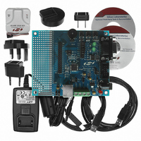
DEV KIT FOR C8051F320/F321
Manufacturer
Silicon Laboratories Inc
Type
MCUr
Specifications of C8051F320DK
Contents
Evaluation Board, Power Supply, USB Cables, Adapter and Documentation
Processor To Be Evaluated
C8051F320/F321
Interface Type
USB
Silicon Manufacturer
Silicon Labs
Core Architecture
8051
Silicon Core Number
C8051F320
Silicon Family Name
C8051F32x
Lead Free Status / RoHS Status
Contains lead / RoHS non-compliant
For Use With/related Products
Silicon Laboratories C8051F320, C8051F321
Lead Free Status / Rohs Status
Lead free / RoHS Compliant
Other names
336-1260
Available stocks
Company
Part Number
Manufacturer
Quantity
Price
Company:

Part Number:
C8051F320DK
Manufacturer:
SiliconL
Quantity:
4


C8051F320/1
17. UART0
18. Enhanced Serial Peripheral Interface (SPI0)
19. Timers
10
Figure 16.2. Typical SMBus Configuration ............................................................. 170
Figure 16.3. SMBus Transaction ............................................................................ 171
Table 16.1. SMBus Clock Source Selection........................................................... 173
Figure 16.4. Typical SMBus SCL Generation......................................................... 174
Table 16.2. Minimum SDA Setup and Hold Times ................................................. 174
Table 16.3. Sources for Hardware Changes to SMB0CN ...................................... 178
Figure 16.5. Typical Master Transmitter Sequence................................................ 180
Figure 16.6. Typical Master Receiver Sequence.................................................... 181
Figure 16.7. Typical Slave Receiver Sequence...................................................... 182
Figure 16.8. Typical Slave Transmitter Sequence.................................................. 183
Table 16.4. SMBus Status Decoding...................................................................... 184
Figure 17.1. UART0 Block Diagram ....................................................................... 187
Figure 17.2. UART0 Baud Rate Logic .................................................................... 188
Figure 17.3. UART Interconnect Diagram .............................................................. 189
Figure 17.4. 8-Bit UART Timing Diagram............................................................... 189
Figure 17.5. 9-Bit UART Timing Diagram............................................................... 190
Figure 17.6. UART Multi-Processor Mode Interconnect Diagram .......................... 191
Table 17.1. Timer Settings for Standard Baud Rates Using The Internal Oscillator ....
Figure 18.1. SPI Block Diagram ............................................................................. 195
Figure 18.2. Multiple-Master Mode Connection Diagram ....................................... 198
Figure 18.3. 3-Wire Single Master and Slave Mode Connection Diagram ............. 198
Figure 18.4. 4-Wire Single Master Mode and 4-Wire Slave Mode Connection Diagram
Figure 18.5. Master Mode Data/Clock Timing ........................................................ 200
Figure 18.6. Slave Mode Data/Clock Timing (CKPHA = 0) .................................... 200
Figure 18.7. Slave Mode Data/Clock Timing (CKPHA = 1) .................................... 201
Figure 18.8. SPI Master Timing (CKPHA = 0)........................................................ 206
Figure 18.9. SPI Master Timing (CKPHA = 1)........................................................ 206
Figure 18.10. SPI Slave Timing (CKPHA = 0)........................................................ 207
Figure 18.11. SPI Slave Timing (CKPHA = 1)........................................................ 207
Table 18.1. SPI Slave Timing Parameters ............................................................. 208
Figure 19.1. T0 Mode 0 Block Diagram.................................................................. 210
Figure 19.2. T0 Mode 2 Block Diagram.................................................................. 211
Figure 19.3. T0 Mode 3 Block Diagram.................................................................. 212
Figure 19.4. Timer 2 16-Bit Mode Block Diagram .................................................. 217
Figure 19.5. Timer 2 8-Bit Mode Block Diagram .................................................... 218
Figure 19.6. Timer 2 SOF Capture Mode (T2SPLIT = ‘0’)...................................... 219
Figure 19.7. Timer 2 SOF Capture Mode (T2SPLIT = ‘1’)...................................... 219
Figure 19.8. Timer 3 16-Bit Mode Block Diagram .................................................. 222
Figure 19.9. Timer 3 8-Bit Mode Block Diagram .................................................... 223
Figure 19.10. Timer 3 SOF Capture Mode (T3SPLIT = ‘0’).................................... 224
194
198
Rev. 1.4
Related parts for C8051F320DK
Image
Part Number
Description
Manufacturer
Datasheet
Request
R

Part Number:
Description:
SMD/C°/SINGLE-ENDED OUTPUT SILICON OSCILLATOR
Manufacturer:
Silicon Laboratories Inc
Part Number:
Description:
Manufacturer:
Silicon Laboratories Inc
Datasheet:
Part Number:
Description:
N/A N/A/SI4010 AES KEYFOB DEMO WITH LCD RX
Manufacturer:
Silicon Laboratories Inc
Datasheet:
Part Number:
Description:
N/A N/A/SI4010 SIMPLIFIED KEY FOB DEMO WITH LED RX
Manufacturer:
Silicon Laboratories Inc
Datasheet:
Part Number:
Description:
N/A/-40 TO 85 OC/EZLINK MODULE; F930/4432 HIGH BAND (REV E/B1)
Manufacturer:
Silicon Laboratories Inc
Part Number:
Description:
EZLink Module; F930/4432 Low Band (rev e/B1)
Manufacturer:
Silicon Laboratories Inc
Part Number:
Description:
I°/4460 10 DBM RADIO TEST CARD 434 MHZ
Manufacturer:
Silicon Laboratories Inc
Part Number:
Description:
I°/4461 14 DBM RADIO TEST CARD 868 MHZ
Manufacturer:
Silicon Laboratories Inc
Part Number:
Description:
I°/4463 20 DBM RFSWITCH RADIO TEST CARD 460 MHZ
Manufacturer:
Silicon Laboratories Inc
Part Number:
Description:
I°/4463 20 DBM RADIO TEST CARD 868 MHZ
Manufacturer:
Silicon Laboratories Inc
Part Number:
Description:
I°/4463 27 DBM RADIO TEST CARD 868 MHZ
Manufacturer:
Silicon Laboratories Inc
Part Number:
Description:
I°/4463 SKYWORKS 30 DBM RADIO TEST CARD 915 MHZ
Manufacturer:
Silicon Laboratories Inc
Part Number:
Description:
N/A N/A/-40 TO 85 OC/4463 RFMD 30 DBM RADIO TEST CARD 915 MHZ
Manufacturer:
Silicon Laboratories Inc
Part Number:
Description:
I°/4463 20 DBM RADIO TEST CARD 169 MHZ
Manufacturer:
Silicon Laboratories Inc