C8051F320DK Silicon Laboratories Inc, C8051F320DK Datasheet - Page 89
C8051F320DK
Manufacturer Part Number
C8051F320DK
Description
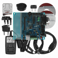
DEV KIT FOR C8051F320/F321
Manufacturer
Silicon Laboratories Inc
Type
MCUr
Specifications of C8051F320DK
Contents
Evaluation Board, Power Supply, USB Cables, Adapter and Documentation
Processor To Be Evaluated
C8051F320/F321
Interface Type
USB
Silicon Manufacturer
Silicon Labs
Core Architecture
8051
Silicon Core Number
C8051F320
Silicon Family Name
C8051F32x
Lead Free Status / RoHS Status
Contains lead / RoHS non-compliant
For Use With/related Products
Silicon Laboratories C8051F320, C8051F321
Lead Free Status / Rohs Status
Lead free / RoHS Compliant
Other names
336-1260
Available stocks
Company
Part Number
Manufacturer
Quantity
Price
Company:

Part Number:
C8051F320DK
Manufacturer:
SiliconL
Quantity:
4


9.3.4. Interrupt Latency
Interrupt response time depends on the state of the CPU when the interrupt occurs. Pending interrupts are
sampled and priority decoded each system clock cycle. Therefore, the fastest possible response time is 5
system clock cycles: 1 clock cycle to detect the interrupt and 4 clock cycles to complete the LCALL to the
ISR. If an interrupt is pending when a RETI is executed, a single instruction is executed before an LCALL
is made to service the pending interrupt. Therefore, the maximum response time for an interrupt (when no
other interrupt is currently being serviced or the new interrupt is of greater priority) occurs when the CPU is
performing an RETI instruction followed by a DIV as the next instruction. In this case, the response time is
18 system clock cycles: 1 clock cycle to detect the interrupt, 5 clock cycles to execute the RETI, 8 clock
cycles to complete the DIV instruction and 4 clock cycles to execute the LCALL to the ISR. If the CPU is
executing an ISR for an interrupt with equal or higher priority, the new interrupt will not be serviced until the
current ISR completes, including the RETI and following instruction.
Note that the CPU is stalled during Flash write/erase operations and USB FIFO MOVX accesses (see Sec-
tion “12.2. Accessing USB FIFO Space” on page 114). Interrupt service latency will be increased for inter-
rupts occuring while the CPU is stalled. The latency for these situations will be determined by the standard
interrupt service procedure (as described above) and the amount of time the CPU is stalled.
Interrupt Source
Reset
External Interrupt 0
(/INT0)
Timer 0 Overflow
External Interrupt 1
(/INT1)
Timer 1 Overflow
UART0
Timer 2 Overflow
SPI0
SMB0
USB0
ADC0 Window
Compare
Interrupt
0x000B
0x001B
0x002B
0x003B
0x004B
0x0000
0x0003
0x0013
0x0023
0x0033
0x0043
Vector
Table 9.4. Interrupt Summary
Priority
Order
Top
0
1
2
3
4
5
6
7
8
9
Pending Flag
None
IE0 (TCON.1)
TF0 (TCON.5)
IE1 (TCON.3)
TF1 (TCON.7)
RI0 (SCON0.0)
TI0 (SCON0.1)
TF2H (TMR2CN.7)
TF2L (TMR2CN.6)
SPIF (SPI0CN.7)
WCOL (SPI0CN.6)
MODF (SPI0CN.5)
RXOVRN
(SPI0CN.4)
SI (SMB0CN.0)
Special
AD0WINT
(ADC0CN.3)
Rev. 1.4
N/A N/A
Y
Y
Y
Y
Y
Y
Y
Y
N
Y
C8051F320/1
Y
Y
Y
Y
N
N
N
N
N
N
Enable
Flag
Always
Enabled
EX0 (IE.0)
ET0 (IE.1) PT0 (IP.1)
EX1 (IE.2)
ET1 (IE.3) PT1 (IP.3)
ES0 (IE.4)
ET2 (IE.5) PT2 (IP.5)
ESPI0
(IE.6)
ESMB0
(EIE1.0)
EUSB0
(EIE1.1)
EWADC0
(EIE1.2)
Priority
Control
Always
Highest
PX0
(IP.0)
PX1
(IP.2)
PS0
(IP.4)
PSPI0
(IP.6)
PSMB0
(EIP1.0)
PUSB0
(EIP1.1)
PWADC0
(EIP1.2)
89
Related parts for C8051F320DK
Image
Part Number
Description
Manufacturer
Datasheet
Request
R

Part Number:
Description:
SMD/C°/SINGLE-ENDED OUTPUT SILICON OSCILLATOR
Manufacturer:
Silicon Laboratories Inc
Part Number:
Description:
Manufacturer:
Silicon Laboratories Inc
Datasheet:
Part Number:
Description:
N/A N/A/SI4010 AES KEYFOB DEMO WITH LCD RX
Manufacturer:
Silicon Laboratories Inc
Datasheet:
Part Number:
Description:
N/A N/A/SI4010 SIMPLIFIED KEY FOB DEMO WITH LED RX
Manufacturer:
Silicon Laboratories Inc
Datasheet:
Part Number:
Description:
N/A/-40 TO 85 OC/EZLINK MODULE; F930/4432 HIGH BAND (REV E/B1)
Manufacturer:
Silicon Laboratories Inc
Part Number:
Description:
EZLink Module; F930/4432 Low Band (rev e/B1)
Manufacturer:
Silicon Laboratories Inc
Part Number:
Description:
I°/4460 10 DBM RADIO TEST CARD 434 MHZ
Manufacturer:
Silicon Laboratories Inc
Part Number:
Description:
I°/4461 14 DBM RADIO TEST CARD 868 MHZ
Manufacturer:
Silicon Laboratories Inc
Part Number:
Description:
I°/4463 20 DBM RFSWITCH RADIO TEST CARD 460 MHZ
Manufacturer:
Silicon Laboratories Inc
Part Number:
Description:
I°/4463 20 DBM RADIO TEST CARD 868 MHZ
Manufacturer:
Silicon Laboratories Inc
Part Number:
Description:
I°/4463 27 DBM RADIO TEST CARD 868 MHZ
Manufacturer:
Silicon Laboratories Inc
Part Number:
Description:
I°/4463 SKYWORKS 30 DBM RADIO TEST CARD 915 MHZ
Manufacturer:
Silicon Laboratories Inc
Part Number:
Description:
N/A N/A/-40 TO 85 OC/4463 RFMD 30 DBM RADIO TEST CARD 915 MHZ
Manufacturer:
Silicon Laboratories Inc
Part Number:
Description:
I°/4463 20 DBM RADIO TEST CARD 169 MHZ
Manufacturer:
Silicon Laboratories Inc