C8051F410DK Silicon Laboratories Inc, C8051F410DK Datasheet - Page 6
C8051F410DK
Manufacturer Part Number
C8051F410DK
Description
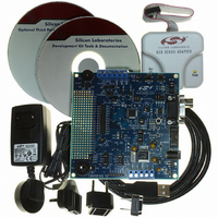
KIT DEV FOR C8051F41X
Manufacturer
Silicon Laboratories Inc
Type
MCUr
Specifications of C8051F410DK
Contents
Evaluation Board, Power Supply, USB Cables, Adapter and Documentation
Processor To Be Evaluated
C8051F41x
Interface Type
USB
Silicon Manufacturer
Silicon Labs
Core Architecture
8051
Silicon Core Number
C8051F410
Silicon Family Name
C8051F41x
Lead Free Status / RoHS Status
Contains lead / RoHS non-compliant
For Use With/related Products
Silicon Laboratories C8051F41x
Lead Free Status / Rohs Status
Lead free / RoHS Compliant
Other names
336-1314
Available stocks
Company
Part Number
Manufacturer
Quantity
Price
Company:

Part Number:
C8051F410DK
Manufacturer:
Silicon Labs
Quantity:
135


C8051F41x-DK
6.1. System Clock Sources
The C8051F410 device installed on the target board features a calibrated programmable internal oscillator which is
enabled as the system clock source on reset. After reset, the internal oscillator operates at a frequency of
191.4 kHz (±2%) by default but may be configured by software to operate at other frequencies. Therefore, in many
applications an external oscillator is not required. However, if you wish to operate the C8051F410 device at a
frequency not available with the internal oscillator, an external crystal may be used. Refer to the C8051F41x data
sheet for more information on configuring the system clock source.
The target board is designed to facilitate the installation of an external crystal. Remove shorting blocks at headers
J9 and J18 and install the crystal at the pads marked Y2. Install a 10 MΩ resistor at R4 and install capacitors at
C44 and C43 using values appropriate for the crystal you select. Refer to the C8051F41x data sheet for more
information on the use of external oscillators. The target board also has a 32.768 kHz watch crystal installed to
provide a timebase for the smaRTClock. Jumper J26 may be used to short the XTAL3 and XTAL4 pins if internal
clock mode is desired.
6.2. Power Options
The C8051F41x Target Board has many power options. This allows the user to exercise the different operating
modes of the C8051F410. The board has 2 voltage regulators. A 3.3 V LDO and a 1.2–5.25 V variable regulator.
To use the 3.3 V regulator, pin 2–3 of J9 should be shorted and a jumper installed in J10.
To use the variable regulator, pin 1–2 of J19 should be shorted and an output voltage should be selected using J21.
After selecting the appropriate voltage, pin 1–2 of J21 should be shorted to enable the output of the variable
regulator. If the voltage "VAR" is selected, the potentiometer R23 should be adjusted until the desired voltage is
reached. The input to the variable regulator can be obtained from the unregulated 9 V supply or from the 5 V USB
VBUS supply available when using a USB debug adapter.
Note: Before enabling either voltage regulator, the user should check the 4 supply rail selection headers
(J29+J30, J17, J12, J31+32) to ensure the correct voltage is being routed to the correct power pin. An
incorrect jumper setting may permanently damage the board. Note that VDD cannot exceed 2.5 V and is
typically derived from the on-chip regulator. Do not connect the 5.25 or 3.3 V output directly to VDD.
The three power LEDs for VIO, VREG, and VDD indicate if the appropriate supply rail is connected to a power
supply. Check to make sure all supply rails (with exception of VREG if not using the on-chip regulator) are
powered.
For the VIO voltage rail, the user may choose from the 3 V regulator (+3 VD), the variable regulator, or the on-chip
regulator. The selections are marked on the target board silkscreen.
For the VREG on-chip voltage regulator input, the user may choose from the 3 V regulator (+3VD), the 5 V USB
VBUS source obtained from the USB debug adapter (5VEC3), or from the variable regulator (VREG). The
selections are marked on the target board silkscreen.
For VDD, the user may choose the output of the on-chip regulator (VDD_) or the output of the variable regulator
(VREG).
6.3. Switches and LEDs
Three switches are provided on the target board. Switch SW1 is connected to the RESET pin of the C8051F410.
Pressing SW1 puts the device into its hardware-reset state. Switch SW2 and SW3 are connected to the
C8051F410’s general purpose I/O (GPIO) pins through headers. Pressing SW2 or SW3 generates a logic low
signal on the port pin. Remove the shorting block from the jumper J5 to disconnect SW2 and/or SW3 from their
associated port pins. The port pin signals are also routed to pins on the J11 I/O connector. See Table 1 for the port
pins and headers corresponding to each switch.
Three LEDs are also provided on the target board. The red LED labeled PWR is used to indicate a power
connection to the target board. The green LEDs labeled with port pin names are connected to the C8051F410’s
GPIO pins through headers. Remove the shorting blocks from the headers to disconnect the LEDs from the port
pins. The port pin signals are also routed to pins on the J1 I/O connector. See Table 1 for the port pins and headers
corresponding to each LED.
6
Rev. 0.2
Related parts for C8051F410DK
Image
Part Number
Description
Manufacturer
Datasheet
Request
R

Part Number:
Description:
SMD/C°/SINGLE-ENDED OUTPUT SILICON OSCILLATOR
Manufacturer:
Silicon Laboratories Inc
Part Number:
Description:
Manufacturer:
Silicon Laboratories Inc
Datasheet:
Part Number:
Description:
N/A N/A/SI4010 AES KEYFOB DEMO WITH LCD RX
Manufacturer:
Silicon Laboratories Inc
Datasheet:
Part Number:
Description:
N/A N/A/SI4010 SIMPLIFIED KEY FOB DEMO WITH LED RX
Manufacturer:
Silicon Laboratories Inc
Datasheet:
Part Number:
Description:
N/A/-40 TO 85 OC/EZLINK MODULE; F930/4432 HIGH BAND (REV E/B1)
Manufacturer:
Silicon Laboratories Inc
Part Number:
Description:
EZLink Module; F930/4432 Low Band (rev e/B1)
Manufacturer:
Silicon Laboratories Inc
Part Number:
Description:
I°/4460 10 DBM RADIO TEST CARD 434 MHZ
Manufacturer:
Silicon Laboratories Inc
Part Number:
Description:
I°/4461 14 DBM RADIO TEST CARD 868 MHZ
Manufacturer:
Silicon Laboratories Inc
Part Number:
Description:
I°/4463 20 DBM RFSWITCH RADIO TEST CARD 460 MHZ
Manufacturer:
Silicon Laboratories Inc
Part Number:
Description:
I°/4463 20 DBM RADIO TEST CARD 868 MHZ
Manufacturer:
Silicon Laboratories Inc
Part Number:
Description:
I°/4463 27 DBM RADIO TEST CARD 868 MHZ
Manufacturer:
Silicon Laboratories Inc
Part Number:
Description:
I°/4463 SKYWORKS 30 DBM RADIO TEST CARD 915 MHZ
Manufacturer:
Silicon Laboratories Inc
Part Number:
Description:
N/A N/A/-40 TO 85 OC/4463 RFMD 30 DBM RADIO TEST CARD 915 MHZ
Manufacturer:
Silicon Laboratories Inc
Part Number:
Description:
I°/4463 20 DBM RADIO TEST CARD 169 MHZ
Manufacturer:
Silicon Laboratories Inc