C8051F410DK Silicon Laboratories Inc, C8051F410DK Datasheet - Page 8
C8051F410DK
Manufacturer Part Number
C8051F410DK
Description
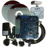
KIT DEV FOR C8051F41X
Manufacturer
Silicon Laboratories Inc
Type
MCUr
Specifications of C8051F410DK
Contents
Evaluation Board, Power Supply, USB Cables, Adapter and Documentation
Processor To Be Evaluated
C8051F41x
Interface Type
USB
Silicon Manufacturer
Silicon Labs
Core Architecture
8051
Silicon Core Number
C8051F410
Silicon Family Name
C8051F41x
Lead Free Status / RoHS Status
Contains lead / RoHS non-compliant
For Use With/related Products
Silicon Laboratories C8051F41x
Lead Free Status / Rohs Status
Lead free / RoHS Compliant
Other names
336-1314
Available stocks
Company
Part Number
Manufacturer
Quantity
Price
Company:

Part Number:
C8051F410DK
Manufacturer:
Silicon Labs
Quantity:
135


C8051F41x-DK
6.5. Target Board DEBUG Interface (J4)
The DEBUG connector (J4) provides access to the DEBUG (C2) pins of the C8051F410. It is used to connect the
Serial Adapter or the USB Debug Adapter to the target board for in-circuit debugging and Flash programming.
Table 3 shows the DEBUG pin definitions.
6.6. Serial Interface (J5)
A RS232 transceiver circuit and DB-9 (J5) connector are provided on the target board to facilitate serial
connections to UART0 of the C8051F410. The TX, RX, RTS and CTS signals of UART0 may be connected to the
DB-9 connector and transceiver by installing shorting blocks on header J3.
6.7. Analog I/O (J6)
Many of the C8051F410 target device’s port pins are connected to the J2 terminal block. Connections for VDDA,
AGND, ADC external voltage references, IDAC outputs and ADC inputs are available. Refer to Table 4 for the J6
terminal block connections.
8
J27[1–2] - Install shorting block to connect UART0 TX (P0.4) to transceiver.
J27[3–4] - Install shorting block to connect UART0 RX (P0.5) to transceiver.
J27[5–6] - Install shorting block to connect UART0 RTS (P1.4) to transceiver.
J27[7–8] - Install shorting block to connect UART0 CTS (P1.5) to transceiver.
Table 3. DEBUG Connector Pin Descriptions
Table 4. J6 Terminal Block Pin Descriptions
2, 3, 9
Pin #
Pin #
10
1
2
3
4
5
6
1
4
5
6
7
8
+3 VD (+3.3 VDC)
Rev. 0.2
Not Connected
GND (Ground)
Description
Description
/RST (Reset)
P0.0/IDAC0
P0.1/IDAC1
USB Power
VREFIN
C2CK
GND
AIN0
AIN1
C2D
P3.0
Related parts for C8051F410DK
Image
Part Number
Description
Manufacturer
Datasheet
Request
R

Part Number:
Description:
SMD/C°/SINGLE-ENDED OUTPUT SILICON OSCILLATOR
Manufacturer:
Silicon Laboratories Inc
Part Number:
Description:
Manufacturer:
Silicon Laboratories Inc
Datasheet:
Part Number:
Description:
N/A N/A/SI4010 AES KEYFOB DEMO WITH LCD RX
Manufacturer:
Silicon Laboratories Inc
Datasheet:
Part Number:
Description:
N/A N/A/SI4010 SIMPLIFIED KEY FOB DEMO WITH LED RX
Manufacturer:
Silicon Laboratories Inc
Datasheet:
Part Number:
Description:
N/A/-40 TO 85 OC/EZLINK MODULE; F930/4432 HIGH BAND (REV E/B1)
Manufacturer:
Silicon Laboratories Inc
Part Number:
Description:
EZLink Module; F930/4432 Low Band (rev e/B1)
Manufacturer:
Silicon Laboratories Inc
Part Number:
Description:
I°/4460 10 DBM RADIO TEST CARD 434 MHZ
Manufacturer:
Silicon Laboratories Inc
Part Number:
Description:
I°/4461 14 DBM RADIO TEST CARD 868 MHZ
Manufacturer:
Silicon Laboratories Inc
Part Number:
Description:
I°/4463 20 DBM RFSWITCH RADIO TEST CARD 460 MHZ
Manufacturer:
Silicon Laboratories Inc
Part Number:
Description:
I°/4463 20 DBM RADIO TEST CARD 868 MHZ
Manufacturer:
Silicon Laboratories Inc
Part Number:
Description:
I°/4463 27 DBM RADIO TEST CARD 868 MHZ
Manufacturer:
Silicon Laboratories Inc
Part Number:
Description:
I°/4463 SKYWORKS 30 DBM RADIO TEST CARD 915 MHZ
Manufacturer:
Silicon Laboratories Inc
Part Number:
Description:
N/A N/A/-40 TO 85 OC/4463 RFMD 30 DBM RADIO TEST CARD 915 MHZ
Manufacturer:
Silicon Laboratories Inc
Part Number:
Description:
I°/4463 20 DBM RADIO TEST CARD 169 MHZ
Manufacturer:
Silicon Laboratories Inc