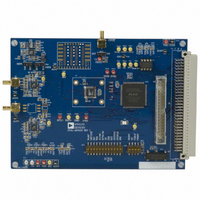
EVAL-AD7655CB Analog Devices Inc, EVAL-AD7655CB Datasheet - Page 4
EVAL-AD7655CB
Manufacturer Part Number
EVAL-AD7655CB
Description
BOARD EVAL FOR AD7655
Manufacturer
Analog Devices Inc
Series
PulSAR®r
Specifications of EVAL-AD7655CB
Number Of Adc's
1
Number Of Bits
16
Sampling Rate (per Second)
1M
Data Interface
Serial, Parallel
Inputs Per Adc
4 Single Ended
Input Range
0 ~ 2 V
Power (typ) @ Conditions
120mW @ 1MSPS
Voltage Supply Source
Analog and Digital
Operating Temperature
-40°C ~ 85°C
Utilized Ic / Part
AD7655
Lead Free Status / RoHS Status
Contains lead / RoHS non-compliant


EVAL-AD76XXCB
R6/(R6+R7)) and U7 at mid-scale from the voltage divider (V
* R29(R29+R60)) for the differential unipolar ADCs.
For the bipolar devices, the input is at 0V (mid-scale). This
allows a transition noise test (histogram) without any other
equipment. In some applications, it is desired to use a bipolar or
wider analog input range, for instance, ± 10V, ± 5V, ± 2.5V, or 0
to -5V. For the AD76XX-48 parts which do not use these input
ranges directly, simple modifications of the input driver
circuitry can be made without any performance degradation.
Refer to the datasheet under the Application Hints section for
component values or to application note
web page for other input ranges.
For dynamic performance, an FFT test can be done by applying
a very low distortion AC source.
POWER SUPPLIES AND GROUNDING
The evaluation board ground plane is separated into two
sections: a plane for the digital interface circuitry and an analog
plane for the analog input and external reference circuitry. To
attain high resolution performance, the board was designed to
ensure that all digital ground return paths do not cross the
analog ground return paths by connecting the planes together
directly under the converter. Power is supplied to the board
through P3 when using with the EVAL-CONTROL-BRDX
USING THE EVAL-AD762X/AD765X/AD766X/
AD767XCB AS STAND-ALONE
Using the evaluation board as stand-alone does not require the
EVAL-CONTROL-BRDX nor does it require use of the
accompanied software. When the CONTROL input to the gate
array is LOW, which is pulled down by default, the gate array
provides the necessary signals for conversion and buffers the
conversion data.
In stand-alone mode, the gate arrays flexible logic buffers the
ADC data according to the read data mode configuration (word
or byte). In parallel reading mode the board is configured for
continuous reading since CS and RD are always driven LOW by
the gate array. Thus, the digital bus is not tri-stated in this mode
of operation and BD[0:15] will continuously be updated after a
new conversion. BD[0:15] is available on P2 after BUSY goes
HIGH. Note that with the 18 bit devices the full 18 bits of data
BD[-2:15] are output directly on P2 since the evaluation board
is not limited to 16 bit wide transfers in stand-alone operation.
When either parallel or serial reading mode, the data is
available on this parallel bus. Refer to Figure 2 to obtain the
data output pins on P2.
Configuration Switches
The evaluation board is configurable for the different operating
modes with 16 positions on the configuration select switches,
S16 and S35. A description of each switch setting and jumper
position is listed in Table 4 and the available test points are
AN594
on the product
Rev. PrW | Page 4 of 22
CM
listed in Table 6. Note that the switches in the ON position
define a logic HIGH level (pulled up with 10kΩ,) and that the
switches are active only in stand-alone mode.
For all interface modes, S16 and S35 allows the selection of:
Warp, Normal or Impulse mode conversions (where applicable)
Binary or 2s complement data output
Reading during or after conversion
Resetting the ADC
ADC power-down
Internal Reference and Buffer power-down (where applicable)
In parallel reading mode, s16 allows the selection of:
Byte swapping for 8 bit interfacing (LSByte with MSByte)
18-bit, 16-bit and 8-bit interfacing (for 18-bit converters)
In serial reading mode, the default settings are Master Read
during Conversion Mode using the internal ADC serial clock.
Serial data is available at T3, T4, T5 and T6 for SDOUT, SCLK,
SYNC and RDERROR respectively. Buffered serial data is
output on the three test points TP17, TP18 and TP19 for SCLK,
SYNC, and SDOUT respectively.
For serial reading mode, S16 allows the selection of:
Choice of inverting SCLK and SYNC
Choice of using internal or external (slave mode) SCLK
SUPPLYING POWER FOR STAND-ALONE USE
Power needs to be supplied through the two power supply
blocks SJ1 and SJ2. Linear supplies are recommended. SJ1 is the
analog supply for the ADC (AVDD), front end op amps and
reference circuitry. SJ2 is the digital supply for the ADC
(DVDD, OVDD) and gate array. The supplies to the device are
configurable through the power supply jumpers shown in
Figure 4 and
Preliminary Technical Data
Related parts for EVAL-AD7655CB
Image
Part Number
Description
Manufacturer
Datasheet
Request
R

Part Number:
Description:
ENERCHIP CC EVAL KIT
Manufacturer:
Cymbet Corporation
Datasheet:

Part Number:
Description:
BOARD EVAL FOR AD976
Manufacturer:
Analog Devices Inc
Datasheet:

Part Number:
Description:
BOARD EVAL FOR ADXL345
Manufacturer:
Analog Devices Inc
Datasheet:

Part Number:
Description:
ENERCHIP CC SEH EVAL KIT
Manufacturer:
Cymbet Corporation
Datasheet:

Part Number:
Description:
ENERCHIP EP ENERGY HARVEST EVAL
Manufacturer:
Cymbet Corporation
Datasheet:

Part Number:
Description:
EVAL BOARD FOR TW6864-LB2-GR
Manufacturer:
Intersil
Datasheet:
Part Number:
Description:
EVAL BOARD FOR TW8816-LB3-GR
Manufacturer:
Intersil
Datasheet:
Part Number:
Description:
EVAL BOARD FOR TW8817-TA3-GRS
Manufacturer:
Intersil
Datasheet:

Part Number:
Description:
EVALUATION MODULE FOR ADUM4160
Manufacturer:
Analog Devices Inc
Datasheet:

Part Number:
Description:
BOARD EVALUATION ADCMP581BCP
Manufacturer:
Analog Devices Inc
Datasheet:
Part Number:
Description:
BOARD EVALUATION ADM1041
Manufacturer:
Analog Devices Inc
Datasheet:

Part Number:
Description:
EVAL BOARD FOR STM32F107VCT
Manufacturer:
STMicroelectronics
Datasheet:
Part Number:
Description:
BOARD EVAL FOR AD1954
Manufacturer:
Analog Devices Inc
Datasheet:
Part Number:
Description:
BOARD EVAL FOR AD1955
Manufacturer:
Analog Devices Inc
Datasheet:

Part Number:
Description:
BOARD EVAL FOR AD9831
Manufacturer:
Analog Devices Inc
Datasheet: