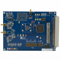
EVAL-AD7655CB Analog Devices Inc, EVAL-AD7655CB Datasheet - Page 16

EVAL-AD7655CB
Manufacturer Part Number
EVAL-AD7655CB
Description
BOARD EVAL FOR AD7655
Manufacturer
Analog Devices Inc
Series
PulSAR®r
Specifications of EVAL-AD7655CB
Number Of Adc's
1
Number Of Bits
16
Sampling Rate (per Second)
1M
Data Interface
Serial, Parallel
Inputs Per Adc
4 Single Ended
Input Range
0 ~ 2 V
Power (typ) @ Conditions
120mW @ 1MSPS
Voltage Supply Source
Analog and Digital
Operating Temperature
-40°C ~ 85°C
Utilized Ic / Part
AD7655
Lead Free Status / RoHS Status
Contains lead / RoHS non-compliant
AD7655
TYPICAL CONNECTION DIAGRAM
Figure 17 shows a typical connection diagram for the AD7655.
Some of the circuitry shown in this diagram is optional and is
discussed in the following sections.
ANALOG INPUTS
Figure 18 shows a simplified analog input section of the
AD7655.
The diodes shown in Figure 18 provide ESD protection for
the inputs. Care must be taken to ensure that the analog input
signal never exceeds the absolute ratings on these inputs.
This causes the diodes to become forward biased and start
conducting current. These diodes can handle a forward-biased
current of 120 mA maximum. This condition can occur when
the input buffer (U1) or (U2) supplies are different from AVDD.
In such a case, an input buffer with a short-circuit current
limitation can be used to protect the part.
This analog input structure allows the sampling of the
differential signal between INx and INxN. Unlike other
converters, the INxN is sampled at the same time as the INx
input. By using differential inputs, small signals common to
both inputs are rejected.
During the acquisition phase, for ac signals, the AD7655
behaves like a one-pole RC filter consisting of the equivalent
resistance R
500 Ω and are a lumped component made up of some serial
resistors and the on resistance of the switches. The C
is typically 32 pF and is mainly the ADC sampling capacitor.
This one-pole filter with a typical −3 dB cutoff frequency of
10 MHz reduces undesirable aliasing effects and limits the
noise coming from the inputs.
Because the input impedance of the AD7655 is very high, the
AD7655 can be driven directly by a low impedance source
without gain error. To further improve the noise filtering of the
AD7655 analog input circuit, an external, one-pole RC filter
between the amplifier output and the ADC input, as shown in
Figure 17, can be used. However, the source impedance has to
INAN
INBN
INA2
INB2
INA1
INB1
A
, R
B
, and C
B
Figure 18. Simplified Analog Input
AGND
AVDD
S
. The resistors R
A0 = L
A0 = H
A0 = L
A0 = H
A0
A
and R
R
R
A
B
C
C
B
S
S
B
are typically
S
capacitor
Rev. B | Page 16 of 28
be kept low because it affects the ac performance, especially the
total harmonic distortion. The maximum source impedance
depends on the amount of total harmonic distortion (THD)
that can be tolerated. The THD degrades when the source
impedance increases.
INPUT CHANNEL MULTIPLEXER
The AD7655 allows the choice of simultaneously sampling the
inputs pairs INA1/INB1 or INA2/INB2 with the A0 multiplexer
input. When A0 is low, the input pairs INA1/INB1 are selected,
and when A0 is high, the input pairs INA2/INB2 are selected.
Note that INAx is always converted before INBx regardless of
the state of the digital interface channel selection A/ B pin.
Also note that the channel selection control, A0, should not be
changed during the acquisition phase of the converter. Refer to
the Conversion Control section and Figure 21 for timing details.
DRIVER AMPLIFIER CHOICE
Although the AD7655 is easy to drive, the driver amplifier
needs to meet at least the following requirements:
•
•
•
The AD8021 meets these requirements and, for almost all
applications, is usually appropriate. The AD8021 needs an
external compensation capacitor of 10 pF. This capacitor should
have good linearity as an NPO ceramic or mica type. The
AD8022 can be used where a dual version is needed and a gain
of +1 is used.
The AD829 is another alternative where high frequency (above
100 kHz) performance is not required. In a gain of +1, it
requires an 82 pF NPO or mica type compensation capacitor.
The AD8610 is another option where low bias current is needed
in low frequency applications.
Refer to Table 8 for some recommended op amps.
The noise generated by the driver amplifier needs to be
kept as low as possible to preserve the SNR and transition
noise performance of the AD7655. The noise coming from
the driver is filtered by the AD7655 analog input circuit
one-pole, low-pass filter made by R
external filter, if one is used.
The driver needs to have a THD performance suitable to
that of the AD7655.
For multichannel, multiplexed applications, the driver
amplifier and the AD7655 analog input circuit together
must be able to settle for a full-scale step of the capacitor
array at a 16-bit level (0.0015%). In the data sheet for the
driver amplifier, the settling at 0.1% or 0.01% is more
commonly specified. This could differ significantly from
the settling time at a 16-bit level and should be verified
prior to driver selection.
A
, R
B
, and C
B
S
or by an


