EVAL-ADUC814QS Analog Devices Inc, EVAL-ADUC814QS Datasheet - Page 32
EVAL-ADUC814QS
Manufacturer Part Number
EVAL-ADUC814QS
Description
KIT DEV FOR ADUC814 QUICK START
Manufacturer
Analog Devices Inc
Series
QuickStart™ Kitr
Type
8052-corer
Datasheet
1.EVAL-ADUC814QSZ.pdf
(72 pages)
Specifications of EVAL-ADUC814QS
Contents
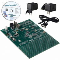
Evaluation Board, Power Supply, Cable, Software and Documentation
For Use With/related Products
ADuC814
Lead Free Status / RoHS Status
Contains lead / RoHS non-compliant


ADuC814
USING FLASH/EE DATA MEMORY
The user Flash/EE data memory array consists of 640 bytes that
are configured into 160 (00H to 9FH) 4-byte pages as shown in
Figure 36.
As with other ADuC814 user-peripheral circuits, the interface
to this memory space is via a group of registers mapped in the
SFR space. EADRL is used to hold the 8-bit address of the page
to be accessed. A group of four data registers (EDATA1–4) is
used to hold 4-byte page data just accessed. Finally, ECON is an
8-bit control register that may be written with one of five
Flash/EE memory access commands to trigger various read,
write, erase, and verify functions. These registers can be
summarized as follows:
ECON
SFR Address
Function
Default
EADRL
SFR Address
Function
Default
EDATA1–4
SFR Address
Function
Default
Table 11. ECON–Flash/EE Memory Control Register Command Modes
Command
Byte
01H
02H
03H
04H
05H
06H
07H to FFH
Figure 36. Flash/EE Data Memory Configuration
9FH
00H
B9H
Controls access to 640 bytes Flash/EE data space.
00H
C6H
Holds the Flash/EE data page address.
(640 bytes = > 160 page addresses)
00H
BCH to BFH, respectively
Holds Flash/EE data memory page write or page
read data bytes.
EDATA1–4 > 00H
Command Mode
READ
PROGRAM
Reserved
VERIFY
ERASE
ERASE-ALL
Reserved
BYTE 1
BYTE 1
BYTE 2 BYTE 3 BYTE 4
BYTE 2 BYTE 3 BYTE 4
Description
Results in 4 bytes being read into EDATA1–4 from memory page address contained in EADRL.
Results in 4 bytes (EDATA1–4) being written to memory page address in EADRL. This write command
assumes the designated write page has been erased.
For internal use. 03H should not be written to the ECON SFR.
Allows the user to verify if data in EDATA1–4 is contained in page address designated by EADRL. A
subsequent read of the ECON SFR results in a zero being read if the verification is valid, a nonzero
value is read to indicate an invalid verification.
Results in an erase of the 4-byte page designated in EADRL.
Results in an erase of the full Flash/EE aata memory, 160-page (640 bytes) array.
For future use.
Rev. A | Page 32 of 72
A block diagram of the SFR interface to the Flash/EE data
memory array is shown in Figure 37.
ECON—Flash/EE Memory Control SFR
This SFR acts as a command interpreter and may be written
with one of five command modes to enable various read,
program, and erase cycles as detailed in Table 11.
FUNCTION:
RECEIVES COMMAND DATA
EADRL
FUNCTION:
HOLDS THE 8-BIT PAGE
ADDRESS POINTER
Figure 37. Flash/EE Data Memory Control and Configuration
9FH
00H
BYTE 1
BYTE 1
INTERPRETER LOGIC
ECON COMMAND
BYTE 2 BYTE 3 BYTE 4
BYTE 2 BYTE 3 BYTE 4
ECON
FUNCTION:
INTERPRETS THE FLASH
COMMAND WORD
FUNCTION:
HOLDS THE 4-BYTE
PAGE DATA
EDATA1 (BYTE 1)
EDATA2 (BYTE 2)
EDATA3 (BYTE 3)
EDATA4 (BYTE 4)
Related parts for EVAL-ADUC814QS
Image
Part Number
Description
Manufacturer
Datasheet
Request
R


Part Number:
Description:
BOARD EVAL FOR SI270X-A
Manufacturer:
Silicon Laboratories Inc
Datasheet:

Part Number:
Description:
BUCK CONV REF DESIGN KIT IP1201
Manufacturer:
International Rectifier
Datasheet:
Part Number:
Description:
BOARD DEMO SYNC DUAL BUCK CNVTER
Manufacturer:
International Rectifier
Datasheet:
Part Number:
Description:
BOARD DEMO SYNC BUCK CONVETER
Manufacturer:
International Rectifier
Datasheet:

Part Number:
Description:
EVALBOARD/EB Omnidirectional microphone - Analog
Manufacturer:
Analog Devices
Datasheet:
Part Number:
Description:
EVALBOARD/EB Omnidirectional microphone - Analog
Manufacturer:
Analog Devices
Datasheet:


Part Number:
Description:
BOARD EVAL LED DRIVER LT3756
Manufacturer:
Linear Technology
Datasheet:

Part Number:
Description:
BOARD EVAL FOR AD7741/7742
Manufacturer:
Analog Devices Inc
Datasheet:

Part Number:
Description:
±1.7g Dual-Axis IMEMS Accelerometer Evaluation Board
Manufacturer:
Analog Devices Inc
Datasheet:

Part Number:
Description:
IC MULTIPLIER ANALOG 8-SOIC T/R
Manufacturer:
Analog Devices Inc
Datasheet:

Part Number:
Description:
IC ANALOG MULTIPLIER 8-DIP
Manufacturer:
Analog Devices Inc
Datasheet:
Part Number:
Description:
IC ANALOG MULTIPLIER 8-SOIC
Manufacturer:
Analog Devices Inc
Datasheet:
Part Number:
Description:
IC ANALOG MULTIPLIER 8-DIP
Manufacturer:
Analog Devices Inc
Datasheet: