EVAL-AD7679CB Analog Devices Inc, EVAL-AD7679CB Datasheet - Page 19
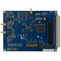
EVAL-AD7679CB
Manufacturer Part Number
EVAL-AD7679CB
Description
BOARD EVAL FOR AD7679
Manufacturer
Analog Devices Inc
Series
PulSAR®r
Specifications of EVAL-AD7679CB
Number Of Adc's
1
Number Of Bits
18
Sampling Rate (per Second)
570k
Data Interface
Serial, Parallel
Inputs Per Adc
1 Differential
Input Range
±VREF
Power (typ) @ Conditions
89mW @ 500kSPS
Voltage Supply Source
Analog and Digital
Operating Temperature
-40°C ~ 85°C
Utilized Ic / Part
AD7679
Lead Free Status / RoHS Status
Contains lead / RoHS non-compliant


Power Supply
The AD7679 uses three sets of power supply pins: an analog 5 V
supply (AVDD), a digital 5 V core supply (DVDD), and a digital
output interface supply (OVDD). The OVDD supply defines
the output logic level and allows direct interface with any logic
working between 2.7 V and DVDD + 0.3 V. To reduce the
number of supplies needed, the digital core (DVDD) can be
supplied through a simple RC filter from the analog supply, as
shown in Figure 25. The AD7679 is independent of power
supply sequencing once OVDD does not exceed DVDD by
more than 0.3 V, and is therefore free from supply voltage
induced latch-up. Additionally, it is very insensitive to power
supply variations over a wide frequency range (see Figure 30).
POWER DISSIPATION VERSUS THROUGHPUT
The AD7679 automatically reduces its power consumption at
the end of each conversion phase. During the acquisition phase,
the operating currents are very low, which allows for a
significant power savings when the conversion rate is reduced,
as shown in Figure 31. This feature makes the AD7679 ideal for
very low power battery applications.
It should be noted that the digital interface remains active even
during the acquisition phase. To reduce the operating digital
supply currents even further, the digital inputs need to be
driven close to the power rails (DVDD and DGND), and
OVDD should not exceed DVDD by more than 0.3 V.
65
60
55
50
45
40
1
Figure 30. PSRR vs. Frequency
10
FREQUECY (kHz)
100
1000
03085-0-032
10000
Rev. A | Page 19 of 28
CONVERSION CONTROL
Figure 32 shows the detailed timing diagrams of the conversion
process. The AD7679 is controlled by the CNVST signal, which
initiates conversion. Once initiated, it cannot be restarted or
aborted, even by PD, until the conversion is complete. The
CNVST signal operates independently of CS and RD .
Although CNVST is a digital signal, it should be designed with
special care with fast, clean edges and levels with minimum
overshoot and undershoot or ringing.
For applications where SNR is critical, the CNVST signal should
have very low jitter. This may be achieved by using a dedicated
oscillator for CNVST generation, or to clock it with a high
frequency low jitter clock, as shown in
For other applications, conversions can be automatically
initiated. If CNVST is held low when BUSY is low, the AD7679
controls the acquisition phase and automatically initiates a new
conversion. By keeping CNVST low, the AD7679 keeps the
conversion process running by itself. It should be noted that the
analog input has to be settled when BUSY goes low. Also, at
power-up, CNVST should be brought low once to initiate the
conversion process. In this mode, the AD7679 could sometimes
run slightly faster than the guaranteed limits of 570 kSPS.
CNVST
MODE
BUSY
1000000
100000
ACQUIRE
10000
1000
100
0.1
10
1
t
t
1
3
5
Figure 31. Power Dissipation vs. Sample Rate
Figure 32. Basic Conversion Timing
t
1
CONVERT
10
t
7
t
4
100
SAMPLING RATE (SPS)
t
t
6
2
1k
ACQUIRE
Figure 25
t
8
10k
.
100k
PDBUF HIGH
AD7679
03085-0-033
CONVERT
03085-0-034
1M
Related parts for EVAL-AD7679CB
Image
Part Number
Description
Manufacturer
Datasheet
Request
R

Part Number:
Description:
ENERCHIP CC EVAL KIT
Manufacturer:
Cymbet Corporation
Datasheet:

Part Number:
Description:
BOARD EVAL FOR AD976
Manufacturer:
Analog Devices Inc
Datasheet:

Part Number:
Description:
BOARD EVAL FOR ADXL345
Manufacturer:
Analog Devices Inc
Datasheet:

Part Number:
Description:
ENERCHIP CC SEH EVAL KIT
Manufacturer:
Cymbet Corporation
Datasheet:

Part Number:
Description:
ENERCHIP EP ENERGY HARVEST EVAL
Manufacturer:
Cymbet Corporation
Datasheet:

Part Number:
Description:
EVAL BOARD FOR TW6864-LB2-GR
Manufacturer:
Intersil
Datasheet:
Part Number:
Description:
EVAL BOARD FOR TW8816-LB3-GR
Manufacturer:
Intersil
Datasheet:
Part Number:
Description:
EVAL BOARD FOR TW8817-TA3-GRS
Manufacturer:
Intersil
Datasheet:

Part Number:
Description:
EVALUATION MODULE FOR ADUM4160
Manufacturer:
Analog Devices Inc
Datasheet:

Part Number:
Description:
BOARD EVALUATION ADCMP581BCP
Manufacturer:
Analog Devices Inc
Datasheet:
Part Number:
Description:
BOARD EVALUATION ADM1041
Manufacturer:
Analog Devices Inc
Datasheet:

Part Number:
Description:
EVAL BOARD FOR STM32F107VCT
Manufacturer:
STMicroelectronics
Datasheet:
Part Number:
Description:
BOARD EVAL FOR AD1954
Manufacturer:
Analog Devices Inc
Datasheet:
Part Number:
Description:
BOARD EVAL FOR AD1955
Manufacturer:
Analog Devices Inc
Datasheet:

Part Number:
Description:
BOARD EVAL FOR AD7655
Manufacturer:
Analog Devices Inc
Datasheet: