EVAL-AD7679CB Analog Devices Inc, EVAL-AD7679CB Datasheet - Page 20
EVAL-AD7679CB
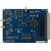
Manufacturer Part Number
EVAL-AD7679CB
Description
BOARD EVAL FOR AD7679
Manufacturer
Analog Devices Inc
Series
PulSAR®r
Specifications of EVAL-AD7679CB
Number Of Adc's
1
Number Of Bits
18
Sampling Rate (per Second)
570k
Data Interface
Serial, Parallel
Inputs Per Adc
1 Differential
Input Range
±VREF
Power (typ) @ Conditions
89mW @ 500kSPS
Voltage Supply Source
Analog and Digital
Operating Temperature
-40°C ~ 85°C
Utilized Ic / Part
AD7679
Lead Free Status / RoHS Status
Contains lead / RoHS non-compliant


AD7679
DIGITAL INTERFACE
The AD7679 has a versatile digital interface; it can be interfaced
with the host system by using either a serial or parallel interface.
The serial interface is multiplexed on the parallel data bus. The
AD7679 digital interface also accommodates both 3 V and 5 V
logic by simply connecting the AD7679’s OVDD supply pin to
the host system interface digital supply. Finally, by using the
OB/ 2C input pin in any mode but 18-bit interface mode, both
twos complement and straight binary coding can be used.
The two signals, CS and RD , control the interface. When at least
one of these signals is high, the interface outputs are in high
impedance. Usually, CS allows the selection of each AD7679 in
multicircuit applications, and is held low in a single AD7679
design. RD is generally used to enable the conversion result on
the data bus.
PARALLEL INTERFACE
The AD7679 is configured to use the parallel interface with an
18-bit, a 16-bit, or an 8-bit bus width, according to Table 7. The
data can be read either after each conversion, which is during
the next acquisition phase, or during the following conversion,
as shown in Figure 35 and Figure 36, respectively. When the
data is read during the conversion, however, it is recommended
that it is read only during the first half of the conversion phase.
This avoids any potential feedthrough between voltage
transients on the digital interface and the most critical analog
CS = RD = 0
CNVST
RESET
Figure 34. Master Parallel Data Timing for Reading (Continuous Read)
BUSY
DATA
BUS
CNVST
BUSY
DATA
BUS
t
3
PREVIOUS CONVERSION DATA
Figure 33. RESET Timing
t
t
1
9
t
10
t
t
8
4
t
11
NEW DATA
03085-0-035
03085-0-036
Rev. A | Page 20 of 28
conversion circuitry. Refer to Table 7 for a detailed description
of the different options available.
SERIAL INTERFACE
The AD7679 is configured to use the serial interface when
MODE0 and MODE1 are held high. The AD7679 outputs 18
bits of data, MSB first, on the SDOUT pin. This data is
synchronized with the 18 clock pulses provided on the SCLK
pin. The output data is valid on both the rising and falling edge
of the data clock.
PINS D[15:8]
PINS D[7:0]
BUSY
DATA
Figure 36. Slave Parallel Data Timing for Reading (Read during Convert)
Figure 35. Slave Parallel Data Timing for Reading (Read after Convert)
CNVST,
BUS
CS = 0
CS
RD
BUSY
DATA
BUS
A0, A1
RD
RD
CS
HI-Z
HI-Z
Figure 37. 8-Bit and 16-Bit Parallel Interface
t
12
t
12
t
3
CONVERSION
CONVERSION
t
PREVIOUS
12
CURRENT
t
HIGH BYTE
LOW BYTE
1
t
t
13
13
t
4
t
12
HIGH BYTE
LOW BYTE
03085-0-039
03085-0-038
03085-0-037
HI-Z
HI-Z
t
13
Related parts for EVAL-AD7679CB
Image
Part Number
Description
Manufacturer
Datasheet
Request
R

Part Number:
Description:
ENERCHIP CC EVAL KIT
Manufacturer:
Cymbet Corporation
Datasheet:

Part Number:
Description:
BOARD EVAL FOR AD976
Manufacturer:
Analog Devices Inc
Datasheet:

Part Number:
Description:
BOARD EVAL FOR ADXL345
Manufacturer:
Analog Devices Inc
Datasheet:

Part Number:
Description:
ENERCHIP CC SEH EVAL KIT
Manufacturer:
Cymbet Corporation
Datasheet:

Part Number:
Description:
ENERCHIP EP ENERGY HARVEST EVAL
Manufacturer:
Cymbet Corporation
Datasheet:

Part Number:
Description:
EVAL BOARD FOR TW6864-LB2-GR
Manufacturer:
Intersil
Datasheet:
Part Number:
Description:
EVAL BOARD FOR TW8816-LB3-GR
Manufacturer:
Intersil
Datasheet:
Part Number:
Description:
EVAL BOARD FOR TW8817-TA3-GRS
Manufacturer:
Intersil
Datasheet:

Part Number:
Description:
EVALUATION MODULE FOR ADUM4160
Manufacturer:
Analog Devices Inc
Datasheet:

Part Number:
Description:
BOARD EVALUATION ADCMP581BCP
Manufacturer:
Analog Devices Inc
Datasheet:
Part Number:
Description:
BOARD EVALUATION ADM1041
Manufacturer:
Analog Devices Inc
Datasheet:

Part Number:
Description:
EVAL BOARD FOR STM32F107VCT
Manufacturer:
STMicroelectronics
Datasheet:
Part Number:
Description:
BOARD EVAL FOR AD1954
Manufacturer:
Analog Devices Inc
Datasheet:
Part Number:
Description:
BOARD EVAL FOR AD1955
Manufacturer:
Analog Devices Inc
Datasheet:

Part Number:
Description:
BOARD EVAL FOR AD7655
Manufacturer:
Analog Devices Inc
Datasheet: