ADC0816CCN/NOPB National Semiconductor, ADC0816CCN/NOPB Datasheet
ADC0816CCN/NOPB
Specifications of ADC0816CCN/NOPB
*ADC0816CCN/NOPB
ADC0816
ADC0816CCN
Available stocks


Related parts for ADC0816CCN/NOPB

ADC0816CCN/NOPB Summary of contents
Page 1
... For similar performance in an 8-channel, 28-pin, 8-bit A/D converter, see the ADC0808, ADC0809 data sheet. (See AN-258 for more in- formation.) Block Diagram TRI-STATE® trademark of National Semiconductor Corporation. © 2007 National Semiconductor Corporation Features ■ Easy interface to all microprocessors ■ ...
Page 2
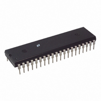
Connection Diagram Ordering Information TEMPERATURE RANGE Error ±½ Bit Unadjusted ±1 Bit Unadjusted Package Outline * This product is obsolete in the Hermetic DIP. www.national.com Dual-In-Line Package Order Number ADC0816CCN or ADC0817CCN See NS Package Number N40A ADC0816CCN ADC0817CCN N40A ...
Page 3
... Absolute Maximum Ratings If Military/Aerospace specified devices are required, please contact the National Semiconductor Sales Office/ Distributors for availability and specifications. Supply Voltage (V ) (Note 3) CC Voltage at Any Pin Except Control Inputs Voltage at Control Inputs (START, OE, CLOCK, ALE, EXPANSION CONTROL, ADD A, ADD B, ADD C, ADD D) ...
Page 4
Symbol Parameter CONTROL INPUTS V Logical “1” Input Voltage IN(1) V Logical “0” Input Voltage IN(0) Logical “1” Input Current I IN(1) (The Control Inputs) I Logical “0” Input Current IN(0) (The Control Inputs) I Supply Current CC ...
Page 5
Functional Description Multiplexer: The device contains a 16-channel single-ended analog signal multiplexer. A particular input channel is select using the address decoder. Table 1 shows the input states for the address line and the expansion control line to ...
Page 6
FIGURE 2. 3-Bit A/D Transfer Curve www.national.com 527703 FIGURE 3. 3-Bit A/D Absolute Accuracy Curve FIGURE 4. Typical Error Curve 6 527704 527705 ...
Page 7
Timing Diagram The successive approximation register (SAR) performs 8 it- erations to approximate the input voltage. For any SAR type converter, n-iterations are required for an n-bit converter. Fig- ure 2 shows a typical example of a 3-bit converter. In ...
Page 8
Typical Performance Characteristics FIGURE 6. Comparator =5V) CC REF TRI-STATE Test Circuits and Timing Diagrams www.national.com 527718 vs FIGURE 8. 8 527719 FIGURE 7. Multiplexer R vs =5V) CC ...
Page 9
Applications Information OPERATION 1.0 Ratiometric Conversion The ADC0816, ADC0817 is designed as a complete Data Acquisition System (DAS) for ratiometric conversion systems. In ratiometric systems, the physical variable being measured is expressed as a percentage of full-scale which is not ...
Page 10
FIGURE 11. Ground Referenced Conversion System with www.national.com FIGURE 10. Ground Referenced Conversion System Using Trimmed Supply Reference Generating V Supply CC FIGURE 12. Typical Reference and Supply Circuit 10 527712 527713 527714 ...
Page 11
Converter Equations The transition between adjacent codes N and given by: (2) The center of an output code N is given by: (3) The output code N for an arbitrary input are the integers within ...
Page 12
Typical Application *Address latches needed for 8085 and SC/MP interfacing the ADC0816 microprocessor Microprocessor Interface Table PROCESSOR 8080 MEMR 8085 RD Z-80 RD SC/MP NRDS VMA•φ 2•R/W 6800 www.national.com READ WRITE INTERRUPT (COMMENT) MEMW INTR (Thru RST ...
Page 13
Physical Dimensions inches (millimeters) unless otherwise noted Molded Dual-In-Line Package (N) NS Package Number N40A 13 www.national.com ...
Page 14
... National Semiconductor and the National Semiconductor logo are registered trademarks of National Semiconductor Corporation. All other brand or product names may be trademarks or registered trademarks of their respective holders. ...