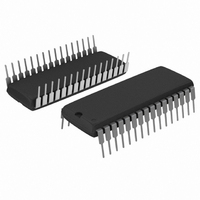
CAT28F020L12 ON Semiconductor, CAT28F020L12 Datasheet

CAT28F020L12
Specifications of CAT28F020L12
CAT28F020L-12
Available stocks
Related parts for CAT28F020L12
CAT28F020L12 Summary of contents
Page 1
... DESCRIPTION The CAT28F020 is a high speed 256K x 8-bit electrically erasable and reprogrammable Flash memory ideally suited for applications requiring in-system or after-sale code updates. Electrical erasure of the full memory contents is achieved typically within 0.5 second pin and Read timing compatible with standard 2 EPROM and E PROM devices ...
Page 2
... I 5115 FHD F01 TSOP Package (Standard Pinout) (T, H) TSOP Package (Reverse Pinout) (TR, HR) 2 Type Function –A Input Address Inputs for 0 17 memory addressing –I/O I/O Data Input/Output 0 7 Input Chip Enable Input Output Enable Input Write Enable Voltage Supply CC Ground ...
Page 3
ABSOLUTE MAXIMUM RATINGS* Temperature Under Bias ................. – +130 C Storage Temperature ....................... – +150 C Voltage on Any Pin with (1) Respect to Ground ........... –2. Voltage on Pin A with 9 (1) ...
Page 4
CAT28F020 D.C. OPERATING CHARACTERISTICS V = +5V 10%, unless otherwise specified. (See Note 2) CC Symbol Parameter I Input Leakage Current LI I Output Leakage Current Standby Current CMOS SB1 Standby Current TTL SB2 ...
Page 5
SUPPLY CHARACTERISTICS ...
Page 6
CAT28F020 A.C. CHARACTERISTICS, Program/Erase Operation V = +5V 10%, unless otherwise specified. (See Note 6) CC JEDEC Standard Symbol Symbol Parameter t t Write Cycle Time AVAV Address Setup Time AVWL Address Hold Time ...
Page 7
FUNCTION TABLE Mode CE Read V IL Output Disable V IL Standby V IH Signature (MFG Signature (Device Program/Erase V IL Write Cycle V IL Read Cycle V IL WRITE COMMAND TABLE Commands are written ...
Page 8
... PP be sent before reading data (see Write Operations). The data retrieved from the I/O pins reflects the contents of the memory location corresponding to the state of the 18 address pins. The respective timing waveforms for the read operation are shown in Figure 3. Refer to the AC Read characteristics for specific timing parameters. ...
Page 9
... In order to commence the erase operation, the identical command of 20H has to be written again into the register. This two-step process ensures against accidental erasure of the memory con- tents. The final erase cycle will be stopped at the rising edge of WE, at which time the Erase Verify command (A0H) is sent to the command register ...
Page 10
CAT28F020 (1) Figure 5. Chip Erase Algorithm START ERASURE APPLY V PPH PROGRAM ALL BYTES TO 00H INITIALIZE ADDRESS INITIALIZE PLSCNT = 0 WRITE ERASE SETUP COMMAND WRITE ERASE COMMAND TIME OUT 10ms WRITE ERASE VERIFY COMMAND TIME OUT 6 ...
Page 11
... Figure 7. During the first write cycle, the command 40H is written into the command register. During the second write cycle, the address of the memory location to be programmed is latched on the falling edge of WE, while the data is latched on the rising edge of WE. The program operation terminates with the next rising edge of WE ...
Page 12
CAT28F020 Figure 7. Programming Algorithm START PROGRAMMING APPLY V PPH INITIALIZE ADDRESS PLSCNT = 0 WRITE SETUP PROG. COMMAND WRITE PROG. CMD ADDR AND DATA TIME OUT 10 s WRITE PROGRAM VERIFY COMMAND TIME OUT 6 s READ DATA FROM ...
Page 13
Abort/Reset An Abort/Reset command is available to allow the user to safely abort an erase or program sequence. Two consecutive program cycles with FFH on the data bus will abort an erase or a program operation. The abort/ reset operation ...
Page 14
CAT28F020 ALTERNATE CE CE CE-CONTROLLED WRITES CE CE JEDEC Standard Symbol Symbol Parameter t t Write Cycle Time AVAV Address Setup Time AVEL Address Hold Time ELAX Data Setup Time DVEH ...
Page 15
EXAMPLE OF ORDERING INFORMATION Prefix Device # CAT 28F020 Product Number Optional Package Company ID N: PLCC T: TSOP (8mmx20mm) TR: TSOP (Reverse Pinout) G: PLCC (Lead free, Halogen free) L: PDIP (Lead free, Halogen free) H: TSOP (Lead free, ...
Page 16
... C Added Green Packages in all areas. 15-Oct-08 D Eliminate PDIP SnPb package. 17-Nov-08 E Change logo and fine print to ON Semiconductor 31-Jul-09 F Update Absolute Maximum Ratings Update Example of Ordering Information Update Ordering Information table ON Semiconductor and are registered trademarks of Semiconductor Components Industries, LLC (SCILLC). SCILLC reserves the right to make changes without further notice to any products herein ...


