ESDA8V2-1MX2 STMicroelectronics, ESDA8V2-1MX2 Datasheet - Page 8
ESDA8V2-1MX2
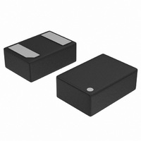
Manufacturer Part Number
ESDA8V2-1MX2
Description
TRANSIL EOS/ESD 8.2V 2QFN
Manufacturer
STMicroelectronics
Datasheet
1.ESDA8V2-1MX2.pdf
(10 pages)
Specifications of ESDA8V2-1MX2
Voltage - Reverse Standoff (typ)
5V
Voltage - Breakdown
8.2V
Power (watts)
500W
Polarization
Unidirectional
Mounting Type
Surface Mount
Package / Case
2-QFN
Polarity
Unidirectional
Channels
1 Channel
Clamping Voltage
12 V, 13 V, 18.5 V
Breakdown Voltage
8.2 V
Termination Style
SMD/SMT
Peak Pulse Power Dissipation
500 W
Capacitance
350 pF
Dimensions
1 mm W x 1.45 mm L x 0.55 mm H
Lead Free Status / RoHS Status
Lead free / RoHS Compliant
Other names
497-10558-2
ESDA8V2-1MX2
ESDA8V2-1MX2
Available stocks
Company
Part Number
Manufacturer
Quantity
Price
Company:

Part Number:
ESDA8V2-1MX2
Manufacturer:
STMicroelectronics
Quantity:
14 300


Recommendation on PCB assembly
4.2
4.3
4.4
8/10
Solder paste
1.
2.
3.
4.
Placement
1.
2.
3.
4.
5.
6.
PCB design preference
1.
2.
Halide-free flux qualification ROL0 according to ANSI/J-STD-004.
“No clean” solder paste is recommended.
Offers a high tack force to resist component movement during high speed
Solder paste with fine particles: powder particle size is 20-45 µm.
Manual positioning is not recommended.
It is recommended to use the lead recognition capabilities of the placement system, not
the outline centering
Standard tolerance of ± 0.05 mm is recommended.
3.5 N placement force is recommended. Too much placement force can lead to
squeezed out solder paste and cause solder joints to short. Too low placement force
can lead to insufficient contact between package and solder paste that could cause
open solder joints or badly centered packages.
To improve the package placement accuracy, a bottom side optical control should be
performed with a high resolution tool.
For assembly, a perfect supporting of the PCB (all the more on flexible PCB) is
recommended during solder paste printing, pick and place and reflow soldering by
using optimized tools.
To control the solder paste amount, the closed via is recommended instead of open
vias.
The position of tracks and open vias in the solder area should be well balanced. The
symmetrical layout is recommended, in case any tilt phenomena caused by
asymmetrical solder paste amount due to the solder flow away.
ESDA8V2-1MX2
Related parts for ESDA8V2-1MX2
Image
Part Number
Description
Manufacturer
Datasheet
Request
R

Part Number:
Description:
TRANSIL EOS/ESD SOD-323
Manufacturer:
STMicroelectronics
Datasheet:

Part Number:
Description:
STMicroelectronics [RIPPLE-CARRY BINARY COUNTER/DIVIDERS]
Manufacturer:
STMicroelectronics
Datasheet:
Part Number:
Description:
STMicroelectronics [LIQUID-CRYSTAL DISPLAY DRIVERS]
Manufacturer:
STMicroelectronics
Datasheet:

Part Number:
Description:
BOARD EVAL FOR MEMS SENSORS
Manufacturer:
STMicroelectronics
Datasheet:
Part Number:
Description:
NPN TRANSISTOR POWER MODULE
Manufacturer:
STMicroelectronics
Datasheet:
Part Number:
Description:
TURBOSWITCH ULTRA-FAST HIGH VOLTAGE DIODE
Manufacturer:
STMicroelectronics
Datasheet:
Part Number:
Description:
Manufacturer:
STMicroelectronics
Datasheet:
Part Number:
Description:
DIODE / SCR MODULE
Manufacturer:
STMicroelectronics
Datasheet:
Part Number:
Description:
DIODE / SCR MODULE
Manufacturer:
STMicroelectronics
Datasheet:
Part Number:
Description:
Search -----> STE16N100
Manufacturer:
STMicroelectronics
Datasheet:
Part Number:
Description:
Search ---> STE53NA50
Manufacturer:
STMicroelectronics
Datasheet:
Part Number:
Description:
NPN Transistor Power Module
Manufacturer:
STMicroelectronics
Datasheet: