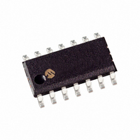
PIC16F526-I/SL Microchip Technology, PIC16F526-I/SL Datasheet - Page 15

PIC16F526-I/SL
Manufacturer Part Number
PIC16F526-I/SL
Description
IC PIC MCU FLASH 1KX12 14SOIC
Manufacturer
Microchip Technology
Series
PIC® 16Fr
Datasheets
1.PIC16F526-ISL.pdf
(122 pages)
2.PIC16F526-ISL.pdf
(22 pages)
3.PIC16F526-IP.pdf
(104 pages)
Specifications of PIC16F526-I/SL
Core Size
8-Bit
Program Memory Size
1.5KB (1K x 12)
Core Processor
PIC
Speed
20MHz
Peripherals
POR, WDT
Number Of I /o
11
Program Memory Type
FLASH
Ram Size
67 x 8
Voltage - Supply (vcc/vdd)
2 V ~ 5.5 V
Data Converters
A/D 3x8b
Oscillator Type
Internal
Operating Temperature
-40°C ~ 85°C
Package / Case
14-SOIC (3.9mm Width), 14-SOL
Controller Family/series
PIC16F
No. Of I/o's
12
Eeprom Memory Size
64Byte
Ram Memory Size
67Byte
Cpu Speed
20MHz
No. Of Timers
1
Processor Series
PIC16F
Core
PIC
Data Bus Width
8 bit
Data Ram Size
67 B
Maximum Clock Frequency
20 MHz
Number Of Programmable I/os
12
Number Of Timers
1
Maximum Operating Temperature
+ 85 C
Mounting Style
SMD/SMT
3rd Party Development Tools
52715-96, 52716-328, 52717-734
Development Tools By Supplier
PG164130, DV164035, DV244005, DV164005, PG164120, ICE2000
Minimum Operating Temperature
- 40 C
On-chip Adc
8 bit, 3 Channel
A/d Bit Size
8 bit
A/d Channels Available
3
Height
1.25 mm
Length
8.65 mm
Supply Voltage (max)
5.5 V
Supply Voltage (min)
2 V
Width
3.9 mm
Lead Free Status / RoHS Status
Lead free / RoHS Compliant
For Use With
ICE2000 - EMULATOR MPLAB-ICE 2000 POD
Eeprom Size
-
Connectivity
-
Lead Free Status / Rohs Status
Details
Available stocks
Company
Part Number
Manufacturer
Quantity
Price
Part Number:
PIC16F526-I/SL
Manufacturer:
MICROCHIP/微芯
Quantity:
20 000
4.0
The PIC16F526 memories are organized into program
memory and data memory (SRAM).The self-writable
portion of the program memory called Flash data
memory is located at addresses at 400h-43Fh. All
Program mode commands that work on the normal
Flash memory work on the Flash data memory. This
includes bulk erase, row/column/cycling toggles, Load
and Read data commands (Refer to Section 5.0
“Flash Data Memory Control” for more details). For
devices with more than 512 bytes of program memory,
a paging scheme is used. Program memory pages are
accessed using one STATUS register bit. For the
PIC16F526, with data memory register files of more
than 32 registers, a banking scheme is used. Data
memory banks are accessed using the File Select
Register (FSR).
4.1
The PIC16F526 device has an 11-bit Program Counter
(PC) capable of addressing a 2K x 12 program memory
space. Program memory is partitioned into user memory,
data memory and configuration memory spaces.
The user memory space is the on-chip user program
memory. As shown in Figure 4-1, it extends from 0x000
to 0x3FF and partitions into pages, including Reset
vector at address 0x3FF.
The data memory space is the Flash data memory
block and is located at addresses PC = 400h-43Fh. All
Program mode commands that work on the normal
Flash memory work on the Flash data memory block.
This includes bulk erase, Load and Read data
commands.
The configuration memory space extends from 0x440
to 0x7FF. Locations from 0x448 through 0x49F are
reserved. The user ID locations extend from 0x440
through 0x443. The Backup OSCCAL locations extend
from 0x444 through 0x447. The Configuration Word is
physically located at 0x7FF.
Refer
Specification” (DS41317) for more details.
2010 Microchip Technology Inc.
to
MEMORY ORGANIZATION
Program Memory Organization for
the PIC16F526
“PIC16F526
Memory
Programming
FIGURE 4-1:
Flash Data Memory
User ID Locations
Configuration Word
Memory (Page 0)
Memory (Page 1)
MEMORY MAP
Backup OSCCAL
Unimplemented
On-chip User
On-chip User
Reserved
Reset Vector
Locations
PIC16F526
Program
Program
DS41326E-page 15
447h
448h
000h
1FFh
200h
3FEh
3FFh
400h
43Fh
440h
443h
444h
4A0h
7FEh
7FFh
49Fh


