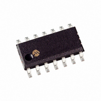
PIC16F526-I/SL Microchip Technology, PIC16F526-I/SL Datasheet - Page 25

PIC16F526-I/SL
Manufacturer Part Number
PIC16F526-I/SL
Description
IC PIC MCU FLASH 1KX12 14SOIC
Manufacturer
Microchip Technology
Series
PIC® 16Fr
Datasheets
1.PIC16F526-ISL.pdf
(122 pages)
2.PIC16F526-ISL.pdf
(22 pages)
3.PIC16F526-IP.pdf
(104 pages)
Specifications of PIC16F526-I/SL
Core Size
8-Bit
Program Memory Size
1.5KB (1K x 12)
Core Processor
PIC
Speed
20MHz
Peripherals
POR, WDT
Number Of I /o
11
Program Memory Type
FLASH
Ram Size
67 x 8
Voltage - Supply (vcc/vdd)
2 V ~ 5.5 V
Data Converters
A/D 3x8b
Oscillator Type
Internal
Operating Temperature
-40°C ~ 85°C
Package / Case
14-SOIC (3.9mm Width), 14-SOL
Controller Family/series
PIC16F
No. Of I/o's
12
Eeprom Memory Size
64Byte
Ram Memory Size
67Byte
Cpu Speed
20MHz
No. Of Timers
1
Processor Series
PIC16F
Core
PIC
Data Bus Width
8 bit
Data Ram Size
67 B
Maximum Clock Frequency
20 MHz
Number Of Programmable I/os
12
Number Of Timers
1
Maximum Operating Temperature
+ 85 C
Mounting Style
SMD/SMT
3rd Party Development Tools
52715-96, 52716-328, 52717-734
Development Tools By Supplier
PG164130, DV164035, DV244005, DV164005, PG164120, ICE2000
Minimum Operating Temperature
- 40 C
On-chip Adc
8 bit, 3 Channel
A/d Bit Size
8 bit
A/d Channels Available
3
Height
1.25 mm
Length
8.65 mm
Supply Voltage (max)
5.5 V
Supply Voltage (min)
2 V
Width
3.9 mm
Lead Free Status / RoHS Status
Lead free / RoHS Compliant
For Use With
ICE2000 - EMULATOR MPLAB-ICE 2000 POD
Eeprom Size
-
Connectivity
-
Lead Free Status / Rohs Status
Details
Available stocks
Company
Part Number
Manufacturer
Quantity
Price
Part Number:
PIC16F526-I/SL
Manufacturer:
MICROCHIP/微芯
Quantity:
20 000
REGISTER 5-3:
5.4
Code protection does not prevent the CPU from
performing read or write operations on the Flash data
memory. Refer to the code protection chapter for more
information.
2010 Microchip Technology Inc.
bit 7
Legend:
S = Bit can only be set
R = Readable bit
-n = Value at POR
bit 7-5
bit 4
bit 3
bit 2
bit 1
bit 0
U-0
—
Code Protection
Unimplemented: Read as ‘0’.
FREE: Flash Data Memory Row Erase Enable Bit
1 = Program memory row being pointed to by EEADR will be erased on the next write cycle. No write
0 = Perform write only
WRERR: Write Error Flag bit
1 = A write operation terminated prematurely (by device Reset)
0 = Write operation completed successfully
WREN: Write Enable bit
1 = Allows write cycle to Flash data memory
0 = Inhibits write cycle to Flash data memory
WR: Write Control bit
1 = Initiate a erase or write cycle
0 = Write/Erase cycle is complete
RD: Read Control bit
1 = Initiate a read of Flash data memory
0 = Do not read Flash data memory
U-0
—
will be performed. This bit is cleared at the completion of the erase operation.
EECON: FLASH CONTROL REGISTER
W = Writable bit
‘1’ = Bit is set
U-0
—
R/W-0
FREE
U = Unimplemented bit, read as ‘0’
‘0’ = Bit is cleared
WRERR
R/W-0
WREN
R/W-0
x = Bit is unknown
PIC16F526
R/W-0
WR
DS41326E-page 25
R/W-0
RD
bit 0


