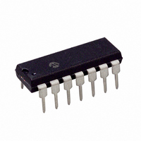
PIC16F505-I/P Microchip Technology, PIC16F505-I/P Datasheet - Page 15

PIC16F505-I/P
Manufacturer Part Number
PIC16F505-I/P
Description
IC MCU FLASH 1KX12 14DIP
Manufacturer
Microchip Technology
Series
PIC® 16Fr
Datasheets
1.PIC12F509T-ISN.pdf
(110 pages)
2.PIC16F505-IST.pdf
(4 pages)
3.PIC16F505-IST.pdf
(22 pages)
4.PIC12F509-EMC.pdf
(106 pages)
Specifications of PIC16F505-I/P
Program Memory Type
FLASH
Program Memory Size
1.5KB (1K x 12)
Package / Case
14-DIP (0.300", 7.62mm)
Core Processor
PIC
Core Size
8-Bit
Speed
20MHz
Peripherals
POR, WDT
Number Of I /o
11
Ram Size
72 x 8
Voltage - Supply (vcc/vdd)
2 V ~ 5.5 V
Oscillator Type
Internal
Operating Temperature
-40°C ~ 85°C
Processor Series
PIC16F
Core
PIC
Data Bus Width
8 bit
Data Ram Size
72 B
Interface Type
RS- 232, USB
Maximum Clock Frequency
20 MHz
Number Of Programmable I/os
12
Number Of Timers
1
Operating Supply Voltage
2 V to 5.5 V
Maximum Operating Temperature
+ 85 C
Mounting Style
Through Hole
3rd Party Development Tools
52715-96, 52716-328, 52717-734
Development Tools By Supplier
PG164130, DV164035, DV244005, DV164005, PG164120, ICE2000
Minimum Operating Temperature
- 40 C
Lead Free Status / RoHS Status
Lead free / RoHS Compliant
For Use With
AC162070 - HEADER INTRFC MPLAB ICD2 8/14PAC162059 - HEADER INTRFC MPLAB ICD2 8/14PINDM163029 - BOARD PICDEM FOR MECHATRONICSDVA16XP140 - ADAPTER DEVICE FOR MPLAB-ICEAC124001 - MODULE SKT PROMATEII 8DIP/SOIC
Eeprom Size
-
Data Converters
-
Connectivity
-
Lead Free Status / Rohs Status
Lead free / RoHS Compliant
TABLE 3-3:
© 2009 Microchip Technology Inc.
RB0/ICSPDAT
RB1/ICSPCLK
RB2
RB3/MCLR/V
RB4/OSC2/CLKOUT
RB5/OSC1/CLKIN
RC0
RC1
RC2
RC3
RC4
RC5/T0CKI
V
V
Legend: I = Input, O = Output, I/O = Input/Output, P = Power, — = Not used, TTL = TTL input,
DD
SS
Name
ST = Schmitt Trigger input, HV = High Voltage
PP
PIC16F505 PINOUT DESCRIPTION
Function
ICSPDAT
ICSPCLK
CLKOUT
CLKIN
MCLR
OSC2
OSC1
T0CKI
RB0
RB1
RB2
RB3
RB4
RB5
RC0
RC1
RC2
RC3
RC4
RC5
V
V
V
DD
PP
SS
Input
XTAL
Type
TTL
TTL
TTL
TTL
TTL
TTL
TTL
TTL
TTL
TTL
TTL
TTL
ST
ST
ST
HV
ST
ST
—
—
—
—
Output
CMOS Bidirectional I/O pin. Can be software programmed for internal
CMOS In-Circuit Serial Programming™ data pin.
CMOS Bidirectional I/O pin. Can be software programmed for internal
CMOS In-Circuit Serial Programming clock pin.
CMOS Bidirectional I/O pin.
CMOS Bidirectional I/O pin. Can be software programmed for internal
CMOS In EXTRC and INTRC modes, the pin output can be
CMOS Bidirectional I/O pin.
CMOS Bidirectional I/O pin.
CMOS Bidirectional I/O pin.
CMOS Bidirectional I/O pin.
CMOS Bidirectional I/O pin.
CMOS Bidirectional I/O pin.
CMOS Bidirectional I/O pin.
XTAL
Type
—
—
—
—
—
—
P
P
weak pull-up and wake-up from Sleep on pin change.
weak pull-up and wake-up from Sleep on pin change.
Input port. Can be software programmed for internal weak
pull-up and wake-up from Sleep on pin change.
Master Clear (Reset). When configured as MCLR, this pin is
an active-low Reset to the device. Voltage on MCLR/V
not exceed V
will enter Programming mode. Weak pull-up always on if
configured as MCLR.
Programming voltage input.
weak pull-up and wake-up from Sleep on pin change.
Oscillator crystal output. Connections to crystal or resonator in
Crystal Oscillator mode (XT, HS and LP modes only).
configured for CLKOUT, which has 1/4 the frequency of OSC1
and denotes the instruction cycle rate.
Crystal input.
External clock source input.
Clock input to TMR0.
Positive supply for logic and I/O pins.
Ground reference for logic and I/O pins.
PIC12F508/509/16F505
DD
during normal device operation or the device
Description
DS41236E-page 15
PP
must


