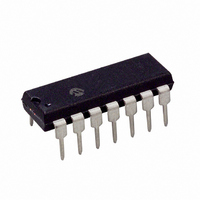
PIC16F505-I/P Microchip Technology, PIC16F505-I/P Datasheet - Page 55

PIC16F505-I/P
Manufacturer Part Number
PIC16F505-I/P
Description
IC MCU FLASH 1KX12 14DIP
Manufacturer
Microchip Technology
Series
PIC® 16Fr
Datasheets
1.PIC12F509T-ISN.pdf
(110 pages)
2.PIC16F505-IST.pdf
(4 pages)
3.PIC16F505-IST.pdf
(22 pages)
4.PIC12F509-EMC.pdf
(106 pages)
Specifications of PIC16F505-I/P
Program Memory Type
FLASH
Program Memory Size
1.5KB (1K x 12)
Package / Case
14-DIP (0.300", 7.62mm)
Core Processor
PIC
Core Size
8-Bit
Speed
20MHz
Peripherals
POR, WDT
Number Of I /o
11
Ram Size
72 x 8
Voltage - Supply (vcc/vdd)
2 V ~ 5.5 V
Oscillator Type
Internal
Operating Temperature
-40°C ~ 85°C
Processor Series
PIC16F
Core
PIC
Data Bus Width
8 bit
Data Ram Size
72 B
Interface Type
RS- 232, USB
Maximum Clock Frequency
20 MHz
Number Of Programmable I/os
12
Number Of Timers
1
Operating Supply Voltage
2 V to 5.5 V
Maximum Operating Temperature
+ 85 C
Mounting Style
Through Hole
3rd Party Development Tools
52715-96, 52716-328, 52717-734
Development Tools By Supplier
PG164130, DV164035, DV244005, DV164005, PG164120, ICE2000
Minimum Operating Temperature
- 40 C
Lead Free Status / RoHS Status
Lead free / RoHS Compliant
For Use With
AC162070 - HEADER INTRFC MPLAB ICD2 8/14PAC162059 - HEADER INTRFC MPLAB ICD2 8/14PINDM163029 - BOARD PICDEM FOR MECHATRONICSDVA16XP140 - ADAPTER DEVICE FOR MPLAB-ICEAC124001 - MODULE SKT PROMATEII 8DIP/SOIC
Eeprom Size
-
Data Converters
-
Connectivity
-
Lead Free Status / Rohs Status
Lead free / RoHS Compliant
7.9
A device may be powered down (Sleep) and later
powered up (wake-up from Sleep).
7.9.1
The Power-Down mode is entered by executing a
SLEEP instruction.
If enabled, the Watchdog Timer will be cleared but
keeps running, the TO bit (STATUS<4>) is set, the PD
bit (STATUS<3>) is cleared and the oscillator driver is
turned off. The I/O ports maintain the status they had
before the SLEEP instruction was executed (driving
high, driving low or high-impedance).
For lowest current consumption while powered down,
the T0CKI input should be at V
(GP3/RB3)/MCLR/V
level if MCLR is enabled.
7.9.2
The device can wake-up from Sleep through one of
the following events:
1.
2.
3.
These events cause a device Reset. The TO, PD and
GPWUF/RBWUF bits can be used to determine the
cause of device Reset. The TO bit is cleared if a WDT
time-out occurred (and caused wake-up). The PD bit,
which is set on power-up, is cleared when SLEEP is
invoked. The GPWUF/RBWUF bit indicates a change
in state while in Sleep at pins GP0/RB0, GP1/RB1,
GP3/RB3 or RB4 (since the last file or bit operation on
GP/RB port).
The WDT is cleared when the device wakes from
Sleep, regardless of the wake-up source.
© 2009 Microchip Technology Inc.
Note:
Note:
An external Reset input on (GP3/RB3)/MCLR/
V
A Watchdog Timer time-out Reset (if WDT was
enabled).
A change on input pin GP0/RB0, GP1/RB1,
GP3/RB3 or RB4 when wake-up on change is
enabled.
PP
pin, when configured as MCLR.
Power-down Mode (Sleep)
SLEEP
A Reset generated by a WDT time-out
does not drive the MCLR pin low.
WAKE-UP FROM SLEEP
Caution: Right before entering Sleep,
read the input pins. When in Sleep, wake-
up occurs when the values at the pins
change from the state they were in at the
last reading. If a wake-up on change
occurs and the pins are not read before re-
entering Sleep, a wake-up will occur
immediately even if no pins change while
in Sleep mode.
PP
pin must be at a logic high
DD
or V
SS
and the
PIC12F508/509/16F505
7.10
If the code protection bit has not been programmed, the
on-chip program memory can be read out for
verification purposes.
The first 64 locations and the last location (OSCCAL)
can be read, regardless of the code protection bit
setting.
The last memory location can be read regardless of the
code protection bit setting on the PIC12F508/509/
16F505 devices.
7.11
Four memory locations are designated as ID locations
where the user can store checksum or other code
identification numbers. These locations are not
accessible during normal execution, but are readable
and writable during Program/Verify.
Use only the lower 4 bits of the ID locations and always
program the upper 8 bits as ‘0’s.
7.12
The PIC12F508/509/16F505 microcontrollers can be
serially programmed while in the end application circuit.
This is simply done with two lines for clock and data,
and three other lines for power, ground and the
programming voltage. This allows customers to manu-
facture boards with unprogrammed devices and then
program the microcontroller just before shipping the
product. This also allows the most recent firmware, or
a custom firmware, to be programmed.
The devices are placed into a Program/Verify mode by
holding the GP1/RB1 and GP0/RB0 pins low while
raising the MCLR (V
programming specification). GP1/RB1 becomes the
programming clock and GP0/RB0 becomes the
programming data. Both GP1/RB1 and GP0/RB0 are
Schmitt Trigger inputs in this mode.
After Reset, a 6-bit command is then supplied to the
device. Depending on the command, 14 bits of program
data are then supplied to or from the device, depending
if the command was a Load or a Read. For complete
details of serial programming, please refer to the
PIC12F508/509/16F505 Programming Specifications.
A typical In-Circuit Serial Programming connection is
shown in Figure 7-15.
Program Verification/Code
Protection
ID Locations
In-Circuit Serial Programming™
PP
) pin from V
DS41236E-page 55
IL
to V
IHH
(see


