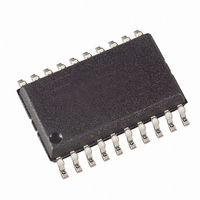
AT89LP4052-20SU Atmel, AT89LP4052-20SU Datasheet - Page 3

AT89LP4052-20SU
Manufacturer Part Number
AT89LP4052-20SU
Description
IC 8051 MCU FLASH 4K 20SOIC
Manufacturer
Atmel
Series
89LPr
Datasheet
1.AT89LP2052-20PU.pdf
(94 pages)
Specifications of AT89LP4052-20SU
Core Processor
8051
Core Size
8-Bit
Speed
20MHz
Connectivity
SPI, UART/USART
Peripherals
Brown-out Detect/Reset, POR, PWM, WDT
Number Of I /o
15
Program Memory Size
4KB (4K x 8)
Program Memory Type
FLASH
Ram Size
256 x 8
Voltage - Supply (vcc/vdd)
2.4 V ~ 5.5 V
Oscillator Type
Internal
Operating Temperature
-40°C ~ 85°C
Package / Case
20-SOIC (7.5mm Width)
Processor Series
AT89x
Core
8051
Data Bus Width
8 bit
Data Ram Size
256 B
Interface Type
SPI/UART
Maximum Clock Frequency
20 MHz
Number Of Programmable I/os
15
Number Of Timers
2
Operating Supply Voltage
2.4 V to 5.5 V
Maximum Operating Temperature
+ 85 C
Mounting Style
SMD/SMT
3rd Party Development Tools
PK51, CA51, A51, ULINK2
Development Tools By Supplier
AT89ISP
Minimum Operating Temperature
- 40 C
Package
20SOIC W
Device Core
8051
Family Name
AT89
Maximum Speed
20 MHz
Lead Free Status / RoHS Status
Lead free / RoHS Compliant
Eeprom Size
-
Data Converters
-
Lead Free Status / Rohs Status
Lead free / RoHS Compliant
Available stocks
Company
Part Number
Manufacturer
Quantity
Price
Company:
Part Number:
AT89LP4052-20SU
Manufacturer:
ATMEL
Quantity:
3 100
3. Pin Description
3547J–MICRO–10/09
Pin
10
11
12
13
14
15
16
17
18
19
20
1
2
3
4
5
6
7
8
9
Symbol
XTAL2
XTAL1
GND
VCC
RST
P3.0
P3.1
P3.2
P3.3
P3.4
P3.5
P3.7
P1.0
P1.1
P1.2
P1.3
P1.4
P1.5
P1.6
P1.7
Type
I/O
I/O
I/O
I/O
I/O
I/O
I/O
I/O
I/O
I/O
I/O
I/O
I/O
I/O
I/O
I/O
I/O
I/O
I/O
I/O
O
O
O
I
I
I
I
I
I
I
I
I
I
I
Description
RST: External Active-High Reset input.
VPP: Parallel Programming Voltage. Raise to 12V to enable programming.
P3.0: User-configurable I/O Port 3 bit 0.
RXD: Serial Port Receiver input.
P3.1: User-configurable I/O Port 3 bit 1.
TXD: Serial Port Transmitter output.
XTAL2: Output from inverting oscillator amplifier.
XTAL1: Input to the inverting oscillator amplifier and internal clock generation circuits.
P3.2: User-configurable I/O Port 3 bit 2.
INT0: External Interrupt 0 input.
P3.3: User-configurable I/O Port 3 bit 3.
INT1: External Interrupt 1input.
P3.4: User-configurable I/O Port 3 bit 4.
T0: Timer 0 Counter input or PWM output
P3.5: User-configurable I/O Port 3 bit 5.
T1: Timer 1 Counter input or PWM output
Ground
P3.7: User-configurable I/O Port 3 bit 7.
SYSCLK: System Clock Output when System Clock Fuse is enabled.
P1.0: User-configurable I/O Port 1 bit 0.
AIN0: Analog Comparator Positive input.
P1.1: User-configurable I/O Port 1 bit 1.
AIN1: Analog Comparator Negative input.
P1.2: User-configurable I/O Port 1 bit 2.
P1.3: User-configurable I/O Port 1 bit 3
P1.4: User-configurable I/O Port 1 bit 4.
SS: SPI slave select.
P1.5: User-configurable I/O Port 1 bit 5.
MOSI: SPI master-out/slave-in. When configured as master, this pin is an output. When configured as
slave, this pin is an input.
P1.6: User-configurable I/O Port 1 bit 6.
MISO: SPI master-in/slave-out. When configured as master, this pin is an input. When configured
as slave, this pin is an output.
P1.7: User-configurable I/O Port 1 bit 7.
SCK: SPI Clock. When configured as master, this pin is an output. When configured as slave, this pin is
an input.
Supply Voltage
AT89LP2052/LP4052
3


