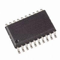
AT89LP4052-20SU Atmel, AT89LP4052-20SU Datasheet - Page 8

AT89LP4052-20SU
Manufacturer Part Number
AT89LP4052-20SU
Description
IC 8051 MCU FLASH 4K 20SOIC
Manufacturer
Atmel
Series
89LPr
Datasheet
1.AT89LP2052-20PU.pdf
(94 pages)
Specifications of AT89LP4052-20SU
Core Processor
8051
Core Size
8-Bit
Speed
20MHz
Connectivity
SPI, UART/USART
Peripherals
Brown-out Detect/Reset, POR, PWM, WDT
Number Of I /o
15
Program Memory Size
4KB (4K x 8)
Program Memory Type
FLASH
Ram Size
256 x 8
Voltage - Supply (vcc/vdd)
2.4 V ~ 5.5 V
Oscillator Type
Internal
Operating Temperature
-40°C ~ 85°C
Package / Case
20-SOIC (7.5mm Width)
Processor Series
AT89x
Core
8051
Data Bus Width
8 bit
Data Ram Size
256 B
Interface Type
SPI/UART
Maximum Clock Frequency
20 MHz
Number Of Programmable I/os
15
Number Of Timers
2
Operating Supply Voltage
2.4 V to 5.5 V
Maximum Operating Temperature
+ 85 C
Mounting Style
SMD/SMT
3rd Party Development Tools
PK51, CA51, A51, ULINK2
Development Tools By Supplier
AT89ISP
Minimum Operating Temperature
- 40 C
Package
20SOIC W
Device Core
8051
Family Name
AT89
Maximum Speed
20 MHz
Lead Free Status / RoHS Status
Lead free / RoHS Compliant
Eeprom Size
-
Data Converters
-
Lead Free Status / Rohs Status
Lead free / RoHS Compliant
Available stocks
Company
Part Number
Manufacturer
Quantity
Price
Company:
Part Number:
AT89LP4052-20SU
Manufacturer:
ATMEL
Quantity:
3 100
7.7
7.8
8. Enhanced CPU
8
I/O Ports
Reset
AT89LP2052/LP4052
The I/O ports of the AT89LP2052/LP4052 may be configured in four different modes. On the
AT89LP2052/LP4052, all the I/O ports revert to input-only (tri-stated) mode at power-up or reset.
In the standard 8051, all ports are weakly pulled high during power-up or reset. To enable 8051-
like ports, the ports must be put into quasi-bidirectional mode by clearing the P1M0 and P3M0
SFRs.
The RST pin in the AT89LP2052/LP4052 has different pulse width requirements than the stan-
dard 8051. The RST pin is sampled every clock cycle and must be held high for a minimum of
two clock cycles, instead of 24 clock cycles, to be recognized as a valid reset pulse
The AT89LP2052/LP4052 uses an enhanced 8051 CPU that runs at 6 to 12 times the speed of
standard 8051 devices (or 3 to 6 times the speed of X2-mode 8051 devices). The increase in
performance is due to two factors. First, the CPU fetches one instruction byte from the code
memory every clock cycle. Second, the CPU uses a simple two-stage pipeline to fetch and exe-
cute instructions in parallel. This basic pipelining concept allows the CPU to obtain up to 1 MIPS
per MHz. A simple example is shown in
The MCS-51 instruction set allows for instructions of variable length from 1 to 3 bytes. In a sin-
gle-clock-per-byte-fetch system this means each instruction takes at least as many clocks as it
has bytes to execute. A majority of the instructions in the AT89LP2052/LP4052 follow this rule:
the instruction execution time in clock cycles equals the number of bytes per instruction with a
few exceptions. Branches and Calls require an additional cycle to compute the target address
and some other complex instructions require multiple cycles. See
Summary” on page 52
8-3
Figure 8-1.
show examples of one- and two-byte instructions.
(n+1)
(n+2)
Parallel Instruction Fetches and Executions
System Clock
n
th
th
th
Instruction
Instruction
Instruction
for more detailed information on individual instructions.
Figure
Fetch
T
n
8-1.
Execute
Fetch
T
n+1
Section 22. “Instruction Set
Execute
Fetch
T
n+2
Figures 8-2 and
3547J–MICRO–10/09


