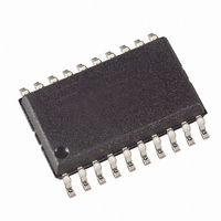
AT89LP4052-20SU Atmel, AT89LP4052-20SU Datasheet - Page 43

AT89LP4052-20SU
Manufacturer Part Number
AT89LP4052-20SU
Description
IC 8051 MCU FLASH 4K 20SOIC
Manufacturer
Atmel
Series
89LPr
Datasheet
1.AT89LP2052-20PU.pdf
(94 pages)
Specifications of AT89LP4052-20SU
Core Processor
8051
Core Size
8-Bit
Speed
20MHz
Connectivity
SPI, UART/USART
Peripherals
Brown-out Detect/Reset, POR, PWM, WDT
Number Of I /o
15
Program Memory Size
4KB (4K x 8)
Program Memory Type
FLASH
Ram Size
256 x 8
Voltage - Supply (vcc/vdd)
2.4 V ~ 5.5 V
Oscillator Type
Internal
Operating Temperature
-40°C ~ 85°C
Package / Case
20-SOIC (7.5mm Width)
Processor Series
AT89x
Core
8051
Data Bus Width
8 bit
Data Ram Size
256 B
Interface Type
SPI/UART
Maximum Clock Frequency
20 MHz
Number Of Programmable I/os
15
Number Of Timers
2
Operating Supply Voltage
2.4 V to 5.5 V
Maximum Operating Temperature
+ 85 C
Mounting Style
SMD/SMT
3rd Party Development Tools
PK51, CA51, A51, ULINK2
Development Tools By Supplier
AT89ISP
Minimum Operating Temperature
- 40 C
Package
20SOIC W
Device Core
8051
Family Name
AT89
Maximum Speed
20 MHz
Lead Free Status / RoHS Status
Lead free / RoHS Compliant
Eeprom Size
-
Data Converters
-
Lead Free Status / Rohs Status
Lead free / RoHS Compliant
Available stocks
Company
Part Number
Manufacturer
Quantity
Price
Company:
Part Number:
AT89LP4052-20SU
Manufacturer:
ATMEL
Quantity:
3 100
3547J–MICRO–10/09
The interconnection between master and slave CPUs with SPI is shown in
pins in the interface are Master-In/Slave-Out (MISO), Master-Out/Slave-In (MOSI), Shift Clock
(SCK), and Slave Select (SS). The SCK pin is the clock output in master mode, but is the clock
input in slave mode. The MSTR bit in SPCR determines the directions of MISO and MOSI. Also
notice that MOSI connects to MOSI and MISO to MISO. In master mode, SS/P1.4 is ignored and
may be used as a general-purpose input or output. In slave mode, SS must be driven low to
select an individual device as a slave. When SS is driven high, the slave’s SPI port is deacti-
vated and the MOSI/P1.5 pin can be used as a general-purpose input.
Figure 19-1. SPI Master-Slave Interconnection
Figure 19-2. SPI Block Diagram
Clock Generator
÷4÷8÷32÷64
SPI
SPI Status Register
Oscillator
Select
Divider
MSB
SPI Control
8-Bit Shift Register
SPI Clock (Mater)
Master
SPI Interrupt
Request
MSTR
SPE
8
LSB
MSB
Data Bus
Internal
8
8-bit Shift Register
Read Data Buffer
Write Data Buffer
8
MISO
MOSI MOSI
SCK
SS
V
CC
SPI Control Register
MISO
SCK
SS
Clock
Logic
AT89LP2052/LP4052
Clock
LSB
MSB
8-Bit Shift Register
S
M
M
S
S
M
Slave
Figure
MISO
MOSI
19-1. The four
P1.6
P1.5
SCK
P1.4
1.7
SS
LSB
43


