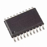
AT89LP4052-20SU Atmel, AT89LP4052-20SU Datasheet - Page 47

AT89LP4052-20SU
Manufacturer Part Number
AT89LP4052-20SU
Description
IC 8051 MCU FLASH 4K 20SOIC
Manufacturer
Atmel
Series
89LPr
Datasheet
1.AT89LP2052-20PU.pdf
(94 pages)
Specifications of AT89LP4052-20SU
Core Processor
8051
Core Size
8-Bit
Speed
20MHz
Connectivity
SPI, UART/USART
Peripherals
Brown-out Detect/Reset, POR, PWM, WDT
Number Of I /o
15
Program Memory Size
4KB (4K x 8)
Program Memory Type
FLASH
Ram Size
256 x 8
Voltage - Supply (vcc/vdd)
2.4 V ~ 5.5 V
Oscillator Type
Internal
Operating Temperature
-40°C ~ 85°C
Package / Case
20-SOIC (7.5mm Width)
Processor Series
AT89x
Core
8051
Data Bus Width
8 bit
Data Ram Size
256 B
Interface Type
SPI/UART
Maximum Clock Frequency
20 MHz
Number Of Programmable I/os
15
Number Of Timers
2
Operating Supply Voltage
2.4 V to 5.5 V
Maximum Operating Temperature
+ 85 C
Mounting Style
SMD/SMT
3rd Party Development Tools
PK51, CA51, A51, ULINK2
Development Tools By Supplier
AT89ISP
Minimum Operating Temperature
- 40 C
Package
20SOIC W
Device Core
8051
Family Name
AT89
Maximum Speed
20 MHz
Lead Free Status / RoHS Status
Lead free / RoHS Compliant
Eeprom Size
-
Data Converters
-
Lead Free Status / Rohs Status
Lead free / RoHS Compliant
Available stocks
Company
Part Number
Manufacturer
Quantity
Price
Company:
Part Number:
AT89LP4052-20SU
Manufacturer:
ATMEL
Quantity:
3 100
19.3
3547J–MICRO–10/09
Serial Clock Generator
Figure 19-3. SPI Shift Register Diagram
The CPHA (Clock PHAse), CPOL (Clock POLarity), and SPR (Serial Peripheral clock Rate =
baud rate) bits in SPCR control the shape and rate of SCK. The two SPR bits provide four possi-
ble clock rates when the SPI is in master mode. In slave mode, the SPI will operate at the rate of
the incoming SCK as long as it does not exceed the maximum bit rate. There are also four pos-
sible combinations of SCK phase and polarity with respect to the serial data. CPHA and CPOL
determine which format is used for transmission. The SPI data transfer formats are shown in
Figures 19-4 and
CPOL, and SPR should be set up before the interface is enabled, and the master device should
be enabled before the slave device(s).
Transmit
Serial In
Byte
8
and 19-5. To prevent glitches on SCK from disrupting the interface, CPHA,
MUX
8
2:1
8
Parallel Master
Serial Master
(Write Buffer)
D
CLK
D
CLK
LATCH
LATCH
Q
Q
7
AT89LP2052/LP4052
MUX
2:1
8
Parallel Slave
Serial Slave
(Read Buffer)
D
CLK
D
CLK
LATCH
LATCH
Q
Q
8
Serial Out
Receive
Byte
47


