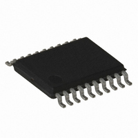
AT89LP4052-20XU Atmel, AT89LP4052-20XU Datasheet - Page 24

AT89LP4052-20XU
Manufacturer Part Number
AT89LP4052-20XU
Description
IC 8051 MCU FLASH 4K 20TSSOP
Manufacturer
Atmel
Series
89LPr
Datasheet
1.AT89LP2052-20PU.pdf
(94 pages)
Specifications of AT89LP4052-20XU
Core Processor
8051
Core Size
8-Bit
Speed
20MHz
Connectivity
SPI, UART/USART
Peripherals
Brown-out Detect/Reset, POR, PWM, WDT
Number Of I /o
15
Program Memory Size
4KB (4K x 8)
Program Memory Type
FLASH
Ram Size
256 x 8
Voltage - Supply (vcc/vdd)
2.4 V ~ 5.5 V
Oscillator Type
Internal
Operating Temperature
-40°C ~ 85°C
Package / Case
20-TSSOP
Processor Series
AT89x
Core
8051
Data Bus Width
8 bit
Data Ram Size
256 B
Interface Type
UART, SPI
Maximum Clock Frequency
20 MHz
Number Of Programmable I/os
15
Number Of Timers
2
Operating Supply Voltage
2.4 V to 5.5 V
Maximum Operating Temperature
+ 85 C
Mounting Style
SMD/SMT
3rd Party Development Tools
PK51, CA51, A51, ULINK2
Development Tools By Supplier
AT89ISP
Minimum Operating Temperature
- 40 C
Package
20TSSOP
Device Core
8051
Family Name
AT89
Maximum Speed
20 MHz
Lead Free Status / RoHS Status
Lead free / RoHS Compliant
Eeprom Size
-
Data Converters
-
Lead Free Status / Rohs Status
Details
16. Enhanced Timer/Counters
16.1
24
Mode 0
AT89LP2052/LP4052
Table 15-4.
The AT89LP2052/LP4052 has two 16-bit Timer/Counter registers: Timer 0 and Timer 1. As a
Timer, the register is incremented every clock cycle. Thus, the register counts clock cycles.
Since a clock cycle consists of one oscillator period, the count rate is equal to the oscillator
frequency.
As a Counter, the register is incremented in response to a 1-to-0 transition at its corresponding
input pin, T0 or T1. The external input is sampled every clock cycle. When the samples show a
high in one cycle and a low in the next cycle, the count is incremented. The new count value
appears in the register during the cycle following the one in which the transition was detected.
Since 2 clock cycles are required to recognize a 1-to-0 transition, the maximum count rate is 1/2
of the oscillator frequency. There are no restrictions on the duty cycle of the input signal, but it
should be held for at least one full clock cycle to ensure that a given level is sampled at least
once before it changes.
Furthermore, the Timer or Counter functions for Timer 0 and Timer 1 have four operating modes:
variable width timer/counter, 16 bit auto-reload timer/counter, 8 bit auto-reload timer/counter,
and split timer/counter. The control bits C/T in the Special Function Register TMOD select the
Timer or Counter function. The bit pairs (M1, M0) in TMOD select the operating modes.
Both Timers in Mode 0 are 8-bit Counters with a variable prescaler. The prescaler may vary from
1 to 8 bits depending on the PSC bits in TCONB, giving the timer a range of 9 to 16 bits.
By default the timer is configured as a 13-bit timer compatible to Mode 0 in the standard 8051.
Figure 16-1
rolls over from all “1”s to all “0”s, it sets the Timer interrupt flag TF1. The counted input is
enabled to the Timer when TR1 = 1 and either GATE = 0 or INT1 = 1. Setting GATE = 1 allows
the Timer to be controlled by external input INT1, to facilitate pulse width measurements. TR1 is
Port
P1.0
P1.1
P1.4
P1.5
P1.6
P1.7
P3.0
P3.1
P3.2
P3.3
P3.4
P3.5
P3.6
Pin
shows the Mode 0 operation as it applies to Timer 1 in 13-bit mode. As the count
Port Pin Alternate Functions
PxM0.y
P1M0.0
P1M0.1
P1M0.4
P1M0.5
P1M0.6
P1M0.7
P3M0.0
P3M0.1
P3M0.2
P3M0.3
P3M0.4
P3M0.5
Configuration Bits
Not configurable
PxM1.y
P1M1.0
P1M1.1
P1M1.4
P1M1.5
P1M1.6
P1M1.7
P3M1.0
P3M1.1
P3M1.2
P3M1.3
P3M1.4
P3M1.5
Alternate
CMPOUT
Function
MOSI
MISO
AIN0
AIN1
INT0
INT1
SCK
RXD
TXD
SS
T0
T1
Notes
Input-only
Input-only
Refer to
Configuration” on page 48
Refer to
Configuration” on page 30
Pin is tied to comparator output
Section 16.6 “Timer/Counter Pin
Section 19.4 “SPI Pin
3547J–MICRO–10/09


