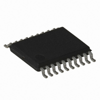
AT89LP4052-20XU Atmel, AT89LP4052-20XU Datasheet - Page 57

AT89LP4052-20XU
Manufacturer Part Number
AT89LP4052-20XU
Description
IC 8051 MCU FLASH 4K 20TSSOP
Manufacturer
Atmel
Series
89LPr
Datasheet
1.AT89LP2052-20PU.pdf
(94 pages)
Specifications of AT89LP4052-20XU
Core Processor
8051
Core Size
8-Bit
Speed
20MHz
Connectivity
SPI, UART/USART
Peripherals
Brown-out Detect/Reset, POR, PWM, WDT
Number Of I /o
15
Program Memory Size
4KB (4K x 8)
Program Memory Type
FLASH
Ram Size
256 x 8
Voltage - Supply (vcc/vdd)
2.4 V ~ 5.5 V
Oscillator Type
Internal
Operating Temperature
-40°C ~ 85°C
Package / Case
20-TSSOP
Processor Series
AT89x
Core
8051
Data Bus Width
8 bit
Data Ram Size
256 B
Interface Type
UART, SPI
Maximum Clock Frequency
20 MHz
Number Of Programmable I/os
15
Number Of Timers
2
Operating Supply Voltage
2.4 V to 5.5 V
Maximum Operating Temperature
+ 85 C
Mounting Style
SMD/SMT
3rd Party Development Tools
PK51, CA51, A51, ULINK2
Development Tools By Supplier
AT89ISP
Minimum Operating Temperature
- 40 C
Package
20TSSOP
Device Core
8051
Family Name
AT89
Maximum Speed
20 MHz
Lead Free Status / RoHS Status
Lead free / RoHS Compliant
Eeprom Size
-
Data Converters
-
Lead Free Status / Rohs Status
Details
23. Programming the Flash Memory
3547J–MICRO–10/09
The AT89LP2052/LP4052 offers 2/4K bytes of In-System Programmable (ISP) non-volatile
Flash code memory. In addition, the device contains a 32-byte User Signature Row and a
32-byte read-only Atmel Signature Row. The memory organization is shown in
Memory is divided into pages of 32 bytes each. A single read or write command may only
access a single page in the memory.
Table 23-1.
The AT89LP2052/LP4052 provides two flexible interfaces for programming the Flash memory: a
parallel interface which uses 10 pins; and a serial interface which uses the 4 SPI pins. The par-
allel and serial programming algorithms are identical. Both interfaces support the same
command format where each command is issued to the device one byte at a time. Commands
consist of a preamble byte for noise immunity, an opcode byte, two address bytes, and from 1 to
32 data bytes.
Figure 23-1. Command Sequence Flow Chart
AT89LP2052
AT89LP4052
Device #
Memory Organization
Figure 23-1
Code Size
2K bytes
4K bytes
shows a simplified flow chart of a command sequence.
Input Preamble
Input Address
Input Address
Input Opcode
Input/Output
High Byte
Low Byte
(AAh)
Data
Page Size
32 bytes
32 bytes
Address +1
AT89LP2052/LP4052
# Pages
128
64
Address Range
0000H - 07FFH
0000H - 0FFFH
Table
23-1. The
57


