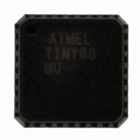
ATTINY88-MU Atmel, ATTINY88-MU Datasheet - Page 27

ATTINY88-MU
Manufacturer Part Number
ATTINY88-MU
Description
MCU AVR 8K ISP FLASH 1.8V 32-QFN
Manufacturer
Atmel
Series
AVR® ATtinyr
Specifications of ATTINY88-MU
Core Processor
AVR
Core Size
8-Bit
Speed
12MHz
Connectivity
I²C, SPI
Peripherals
Brown-out Detect/Reset, POR, WDT
Number Of I /o
28
Program Memory Size
8KB (4K x 16)
Program Memory Type
FLASH
Eeprom Size
64 x 8
Ram Size
512 x 8
Voltage - Supply (vcc/vdd)
1.8 V ~ 5.5 V
Data Converters
A/D 8x10b
Oscillator Type
Internal
Operating Temperature
-40°C ~ 85°C
Package / Case
32-VQFN Exposed Pad, 32-HVQFN, 32-SQFN, 32-DHVQFN
Processor Series
ATTINY8x
Core
AVR8
Data Bus Width
8 bit
Data Ram Size
512 B
Interface Type
2-Wire, I2S, SPI
Maximum Clock Frequency
12 MHz
Number Of Programmable I/os
28
Number Of Timers
2
Maximum Operating Temperature
+ 85 C
Mounting Style
SMD/SMT
3rd Party Development Tools
EWAVR, EWAVR-BL
Development Tools By Supplier
ATAVRDRAGON, ATSTK500, ATSTK600, ATAVRISP2, ATAVRONEKIT, ATQT600, ATAVRTS2080B
Minimum Operating Temperature
- 40 C
On-chip Adc
10 bit, 8 Channel
Package
32QFN EP
Device Core
AVR
Family Name
ATtiny
Maximum Speed
12 MHz
Operating Supply Voltage
2.5|3.3|5 V
Cpu Family
ATtiny
Device Core Size
8b
Frequency (max)
12MHz
Total Internal Ram Size
512Byte
# I/os (max)
28
Number Of Timers - General Purpose
2
Operating Supply Voltage (typ)
2.5/3.3/5V
Operating Supply Voltage (max)
5.5V
Operating Supply Voltage (min)
1.8V
Instruction Set Architecture
RISC
Operating Temp Range
-40C to 85C
Operating Temperature Classification
Industrial
Mounting
Surface Mount
Pin Count
32
Package Type
QFN EP
For Use With
ATSTK600-DIP40 - STK600 SOCKET/ADAPTER 40-PDIPATAVRDRAGON - KIT DRAGON 32KB FLASH MEM AVR
Lead Free Status / RoHS Status
Lead free / RoHS Compliant
Available stocks
Company
Part Number
Manufacturer
Quantity
Price
Company:
Part Number:
ATTINY88-MU
Manufacturer:
ATMEL
Quantity:
21 342
Part Number:
ATTINY88-MU
Manufacturer:
ATMEL/爱特梅尔
Quantity:
20 000
Part Number:
ATTINY88-MUR
Manufacturer:
AT
Quantity:
20 000
- Current page: 27 of 302
- Download datasheet (9Mb)
5.4.4
5.4.5
5.4.6
8008G–AVR–04/11
GPIOR2 – General Purpose I/O Register 2
GPIOR1 – General Purpose I/O Register 1
GPIOR0 – General Purpose I/O Register 0
interrupted EEPROM access to fail. It is recommended to have the Global Interrupt Flag cleared
during all the steps to avoid these problems.
When the write access time has elapsed, the EEPE bit is cleared by hardware. The user soft-
ware can poll this bit and wait for a zero before writing the next byte. When EEPE has been set,
the CPU is halted for two cycles before the next instruction is executed.
• Bit 0 – EERE: EEPROM Read Enable
This is the read strobe of the EEPROM. When the target address has been set up in the EEAR,
the EERE bit must be written to one to trigger the EEPROM read operation.
EEPROM read access takes one instruction, and the requested data is available immediately.
When the EEPROM is read, the CPU is halted for four cycles before the next instruction is
executed.
The user should poll the EEPE bit before starting the read operation. If a write operation is in
progress, it not possible to read the EEPROM, or to change the address register (EEAR).
This register may be used freely for storing any kind of data.
This register may be used freely for storing any kind of data.
This register may be used freely for storing any kind of data.
Bit
0x2B (0x4B)
Read/Write
Initial Value
Bit
0x2A (0x4A)
Read/Write
Initial Value
Bit
0x1E (0x3E)
Read/Write
Initial Value
MSB
MSB
MSB
R/W
R/W
R/W
7
0
7
0
7
0
R/W
R/W
R/W
6
0
6
0
6
0
R/W
R/W
R/W
5
0
5
0
5
0
R/W
R/W
R/W
4
0
4
0
4
0
R/W
R/W
R/W
3
0
3
0
3
0
R/W
R/W
R/W
2
0
2
0
2
0
R/W
R/W
R/W
1
0
1
0
1
0
ATtiny48/88
LSB
R/W
LSB
R/W
LSB
R/W
0
0
0
0
0
0
GPIOR2
GPIOR1
GPIOR0
27
Related parts for ATTINY88-MU
Image
Part Number
Description
Manufacturer
Datasheet
Request
R

Part Number:
Description:
IC, MCU, 8BIT, 2K FLASH, 20SOIC
Manufacturer:
Atmel
Datasheet:

Part Number:
Description:
IC, MCU, 8BIT, 2K FLASH, 20PDIP
Manufacturer:
Atmel
Datasheet:

Part Number:
Description:
IC, MCU, 8BIT, 8K FLASH, 20PDIP
Manufacturer:
Atmel
Datasheet:

Part Number:
Description:
IC, MCU, 8BIT, 8K FLASH, 20SOIC
Manufacturer:
Atmel
Datasheet:

Part Number:
Description:
DEV KIT FOR AVR/AVR32
Manufacturer:
Atmel
Datasheet:

Part Number:
Description:
INTERVAL AND WIPE/WASH WIPER CONTROL IC WITH DELAY
Manufacturer:
ATMEL Corporation
Datasheet:

Part Number:
Description:
Low-Voltage Voice-Switched IC for Hands-Free Operation
Manufacturer:
ATMEL Corporation
Datasheet:

Part Number:
Description:
MONOLITHIC INTEGRATED FEATUREPHONE CIRCUIT
Manufacturer:
ATMEL Corporation
Datasheet:

Part Number:
Description:
AM-FM Receiver IC U4255BM-M
Manufacturer:
ATMEL Corporation
Datasheet:

Part Number:
Description:
Monolithic Integrated Feature Phone Circuit
Manufacturer:
ATMEL Corporation
Datasheet:

Part Number:
Description:
Multistandard Video-IF and Quasi Parallel Sound Processing
Manufacturer:
ATMEL Corporation
Datasheet:

Part Number:
Description:
High-performance EE PLD
Manufacturer:
ATMEL Corporation
Datasheet:


