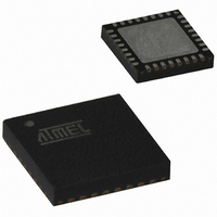
ATTINY461-20MU Atmel, ATTINY461-20MU Datasheet - Page 38

ATTINY461-20MU
Manufacturer Part Number
ATTINY461-20MU
Description
IC AVR MCU 4K 20MHZ 32-QFN
Manufacturer
Atmel
Series
AVR® ATtinyr
Specifications of ATTINY461-20MU
Core Processor
AVR
Core Size
8-Bit
Speed
20MHz
Connectivity
USI
Peripherals
Brown-out Detect/Reset, POR, PWM, WDT
Number Of I /o
16
Program Memory Size
4KB (2K x 16)
Program Memory Type
FLASH
Eeprom Size
256 x 8
Ram Size
256 x 8
Voltage - Supply (vcc/vdd)
2.7 V ~ 5.5 V
Data Converters
A/D 11x10b
Oscillator Type
Internal
Operating Temperature
-40°C ~ 85°C
Package / Case
32-VQFN Exposed Pad, 32-HVQFN, 32-SQFN, 32-DHVQFN
Processor Series
ATTINY4x
Core
AVR8
Data Bus Width
8 bit
Data Ram Size
256 B
Interface Type
2-Wire, SPI, USI
Maximum Clock Frequency
20 MHz
Number Of Programmable I/os
16
Number Of Timers
2
Maximum Operating Temperature
+ 85 C
Mounting Style
SMD/SMT
3rd Party Development Tools
EWAVR, EWAVR-BL
Development Tools By Supplier
ATAVRDRAGON, ATSTK500, ATSTK600, ATAVRISP2, ATAVRONEKIT
Minimum Operating Temperature
- 40 C
On-chip Adc
10 bit, 11 Channel
For Use With
ATSTK600-DIP40 - STK600 SOCKET/ADAPTER 40-PDIPATAVRBC100 - REF DESIGN KIT BATTERY CHARGER770-1007 - ISP 4PORT ATMEL AVR MCU SPI/JTAG
Lead Free Status / RoHS Status
Lead free / RoHS Compliant
Available stocks
Company
Part Number
Manufacturer
Quantity
Price
Company:
Part Number:
ATTINY461-20MU
Manufacturer:
KODENSHI
Quantity:
991
Company:
Part Number:
ATTINY461-20MUR
Manufacturer:
ATMEL
Quantity:
5 560
7.3.1
7.3.2
7.3.3
7.3.4
7.3.5
7.3.6
38
ATtiny261/461/861
Analog Comparator
Analog to Digital Converter
Brown-out Detector
Internal Voltage Reference
Watchdog Timer
Port Pins
When entering Idle mode, the Analog Comparator should be disabled if not used. When entering
ADC Noise Reduction mode, the Analog Comparator should be disabled. In the other sleep
modes, the Analog Comparator is automatically disabled. However, if the Analog Comparator is
set up to use the Internal Voltage Reference as input, the Analog Comparator should be dis-
abled in all sleep modes. Otherwise, the Internal Voltage Reference will be enabled,
independent of sleep mode. Refer to
to configure the Analog Comparator.
If enabled, the ADC will be enabled in all sleep modes. To save power, the ADC should be dis-
abled before entering any sleep mode. When the ADC is turned off and on again, the next
conversion will be an extended conversion. Refer to
page 142
If the Brown-out Detector is not needed in the application, this module should be turned off. If the
Brown-out Detector is enabled by the BODLEVEL Fuses, it will be enabled in all sleep modes,
and hence, always consume power. In the deeper sleep modes, this will contribute significantly
to the total current consumption. Refer to
configure the Brown-out Detector.
The Internal Voltage Reference will be enabled when needed by the Brown-out Detection, the
Analog Comparator or the ADC. If these modules are disabled as described in the sections
above, the internal voltage reference will be disabled and it will not be consuming power. When
turned on again, the user must allow the reference to start up before the output is used. If the
reference is kept on in sleep mode, the output can be used immediately. Refer to
age Reference” on page 44
If the Watchdog Timer is not needed in the application, this module should be turned off. If the
Watchdog Timer is enabled, it will be enabled in all sleep modes, and hence, always consume
power. In the deeper sleep modes, this will contribute significantly to the total current consump-
tion. Refer to
When entering a sleep mode, all port pins should be configured to use minimum power. The
most important thing is then to ensure that no pins drive resistive loads. In sleep modes where
both the I/O clock (clk
will be disabled. This ensures that no power is consumed by the input logic when not needed. In
some cases, the input logic is needed for detecting wake-up conditions, and it will then be
enabled. Refer to the section
which pins are enabled. If the input buffer is enabled and the input signal is left floating or has an
analog signal level close to V
For analog input pins, the digital input buffer should be disabled at all times. An analog signal
level close to V
input buffers can be disabled by writing to the Digital Input Disable Registers (DIDR0, DIDR1).
for details on ADC operation.
“Watchdog Timer” on page 44
CC
/2 on an input pin can cause significant current even in active mode. Digital
I/O
) and the ADC clock (clk
for details on the start-up time.
CC
“Digital Input Enable and Sleep Modes” on page 59
/2, the input buffer will use excessive power.
“AC – Analog Comparator” on page 137
“Brown-out Detection” on page 43
for details on how to configure the Watchdog Timer.
ADC
) are stopped, the input buffers of the device
“ADC – Analog to Digital Converter” on
for details on how to
for details on how
2588E–AVR–08/10
“Internal Volt-
for details on


