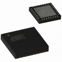
AT90PWM3-16MQ Atmel, AT90PWM3-16MQ Datasheet - Page 233

AT90PWM3-16MQ
Manufacturer Part Number
AT90PWM3-16MQ
Description
IC AVR MCU FLASH 8K 32QFN
Manufacturer
Atmel
Series
AVR® 90PWM Lightingr
Datasheet
1.AT90PWM3B-16SU.pdf
(361 pages)
Specifications of AT90PWM3-16MQ
Core Processor
AVR
Core Size
8-Bit
Speed
16MHz
Connectivity
SPI, UART/USART
Peripherals
Brown-out Detect/Reset, POR, PWM, WDT
Number Of I /o
27
Program Memory Size
8KB (8K x 8)
Program Memory Type
FLASH
Eeprom Size
512 x 8
Ram Size
512 x 8
Voltage - Supply (vcc/vdd)
2.7 V ~ 5.5 V
Data Converters
A/D 11x10b; D/A 1x10b
Oscillator Type
Internal
Operating Temperature
-40°C ~ 105°C
Package / Case
32-QFN
Processor Series
AT90PWMx
Core
AVR8
Data Bus Width
8 bit
Data Ram Size
512 B
Interface Type
SPI, USART
Maximum Clock Frequency
16 MHz
Number Of Programmable I/os
27
Number Of Timers
2
Operating Supply Voltage
2.7 V to 5.5 V
Maximum Operating Temperature
+ 105 C
Mounting Style
SMD/SMT
3rd Party Development Tools
EWAVR, EWAVR-BL
Development Tools By Supplier
ATAVRDRAGON, ATSTK500, ATSTK600, ATAVRISP2, ATAVRONEKIT, ATAVRFBKIT, ATAVRISP2
Minimum Operating Temperature
- 40 C
On-chip Adc
10 bit, 11 Channel
On-chip Dac
10 bit, 1 Channel
For Use With
ATSTK600-SOIC - STK600 SOCKET/ADAPTER FOR SOICATAVRMC200 - KIT EVAL FOR AT90PWM3 ASYNCATAVRFBKIT - KIT DEMO BALLAST FOR AT90PWM2ATAVRISP2 - PROGRAMMER AVR IN SYSTEMATSTK520 - ADAPTER KIT FOR 90PWM
Lead Free Status / RoHS Status
Lead free / RoHS Compliant
Available stocks
Company
Part Number
Manufacturer
Quantity
Price
Company:
Part Number:
AT90PWM3-16MQT
Manufacturer:
Atmel
Quantity:
1 325
- Current page: 233 of 361
- Download datasheet (7Mb)
21. Analog to Digital Converter - ADC
21.1
4317J–AVR–08/10
Features
•
•
•
•
•
•
•
•
•
•
•
•
•
•
The AT90PWM2/2B/3/3B features a 10-bit successive approximation ADC. The ADC is con-
nected to an 15-channel Analog Multiplexer which allows eleven single-ended input. The single-
ended voltage inputs refer to 0V (GND).
The device also supports 2 differential voltage input combinations which are equipped with a
programmable gain stage, providing amplification steps of 14dB (5x), 20 dB (10x), 26 dB (20x),
or 32dB (40x) on the differential input voltage before the A/D conversion. On the amplified chan-
nels, 8-bit resolution can be expected.
The ADC contains a Sample and Hold circuit which ensures that the input voltage to the ADC is
held at a constant level during conversion. A block diagram of the ADC is shown in
The ADC has a separate analog supply voltage pin, AV
0.3V from V
pin.
Internal reference voltages of nominally 2.56V or AV
ence may be externally decoupled at the AREF pin by a capacitor for better noise performance.
10-bit Resolution
0.5 LSB Integral Non-linearity
± 2 LSB Absolute Accuracy
8- 320 µs Conversion Time
Up to 125 kSPS at Maximum Resolution
11 Multiplexed Single Ended Input Channels
Two Differential input channels with accurate programmable gain 5, 10, 20 and 40
Optional Left Adjustment for ADC Result Readout
0 - V
Selectable 2.56 V ADC Reference Voltage
Free Running or Single Conversion Mode
ADC Start Conversion by Auto Triggering on Interrupt Sources
Interrupt on ADC Conversion Complete
Sleep Mode Noise Canceler
CC
ADC Input Voltage Range
CC
. See the paragraph
“ADC Noise Canceler” on page 240
CC
are provided On-chip. The voltage refer-
CC
AT90PWM2/3/2B/3B
. AV
CC
must not differ more than ±
on how to connect this
Figure
21-1.
233
Related parts for AT90PWM3-16MQ
Image
Part Number
Description
Manufacturer
Datasheet
Request
R

Part Number:
Description:
IC AVR MCU FLASH 8K 32SOIC
Manufacturer:
Atmel
Datasheet:

Part Number:
Description:
MCU AVR 8K FLASH 16MHZ 32-QFN
Manufacturer:
Atmel
Datasheet:

Part Number:
Description:
DEV KIT FOR AVR/AVR32
Manufacturer:
Atmel
Datasheet:

Part Number:
Description:
INTERVAL AND WIPE/WASH WIPER CONTROL IC WITH DELAY
Manufacturer:
ATMEL Corporation
Datasheet:

Part Number:
Description:
Low-Voltage Voice-Switched IC for Hands-Free Operation
Manufacturer:
ATMEL Corporation
Datasheet:

Part Number:
Description:
MONOLITHIC INTEGRATED FEATUREPHONE CIRCUIT
Manufacturer:
ATMEL Corporation
Datasheet:

Part Number:
Description:
AM-FM Receiver IC U4255BM-M
Manufacturer:
ATMEL Corporation
Datasheet:

Part Number:
Description:
Monolithic Integrated Feature Phone Circuit
Manufacturer:
ATMEL Corporation
Datasheet:

Part Number:
Description:
Multistandard Video-IF and Quasi Parallel Sound Processing
Manufacturer:
ATMEL Corporation
Datasheet:

Part Number:
Description:
High-performance EE PLD
Manufacturer:
ATMEL Corporation
Datasheet:

Part Number:
Description:
8-bit Flash Microcontroller
Manufacturer:
ATMEL Corporation
Datasheet:

Part Number:
Description:
2-Wire Serial EEPROM
Manufacturer:
ATMEL Corporation
Datasheet:


