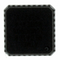
ATMEGA168-20MU Atmel, ATMEGA168-20MU Datasheet - Page 260

ATMEGA168-20MU
Manufacturer Part Number
ATMEGA168-20MU
Description
IC AVR MCU 16K 20MHZ 32-QFN
Manufacturer
Atmel
Series
AVR® ATmegar
Datasheets
1.ATAVRTS2080B.pdf
(378 pages)
2.ATMEGA48-20AU.pdf
(35 pages)
3.ATMEGA88-20MU.pdf
(33 pages)
Specifications of ATMEGA168-20MU
Core Processor
AVR
Core Size
8-Bit
Speed
20MHz
Connectivity
I²C, SPI, UART/USART
Peripherals
Brown-out Detect/Reset, POR, PWM, WDT
Number Of I /o
23
Program Memory Size
16KB (8K x 16)
Program Memory Type
FLASH
Eeprom Size
512 x 8
Ram Size
1K x 8
Voltage - Supply (vcc/vdd)
2.7 V ~ 5.5 V
Data Converters
A/D 8x10b
Oscillator Type
Internal
Operating Temperature
-40°C ~ 85°C
Package / Case
32-VQFN Exposed Pad, 32-HVQFN, 32-SQFN, 32-DHVQFN
Processor Series
ATMEGA16x
Core
AVR8
Data Bus Width
8 bit
Data Ram Size
1 KB
Interface Type
2-Wire, SPI, USART, Serial
Maximum Clock Frequency
20 MHz
Number Of Programmable I/os
23
Number Of Timers
3
Operating Supply Voltage
2.7 V to 5.5 V
Maximum Operating Temperature
+ 85 C
Mounting Style
SMD/SMT
3rd Party Development Tools
EWAVR, EWAVR-BL
Development Tools By Supplier
ATAVRDRAGON, ATSTK500, ATSTK600, ATAVRISP2, ATAVRONEKIT
Minimum Operating Temperature
- 40 C
On-chip Adc
10 bit, 8 Channel
A/d Inputs
8-Channel, 10-Bit
Cpu Speed
20 MIPS
Eeprom Memory
512 Bytes
Input Output
23
Interface
I2C/SPI/UART/USART
Memory Type
Flash
Number Of Bits
8
Package Type
32-pin MLF
Programmable Memory
16K Bytes
Timers
2-8-bit, 1-16-bit
Voltage, Range
4.5-5.5 V
Cpu Family
ATmega
Device Core
AVR
Device Core Size
8b
Frequency (max)
20MHz
Total Internal Ram Size
1KB
# I/os (max)
23
Number Of Timers - General Purpose
3
Operating Supply Voltage (typ)
3.3/5V
Operating Supply Voltage (max)
5.5V
Operating Supply Voltage (min)
2.7V
Instruction Set Architecture
RISC
Operating Temp Range
-40C to 85C
Operating Temperature Classification
Industrial
Mounting
Surface Mount
Pin Count
32
Controller Family/series
AVR MEGA
No. Of I/o's
23
Eeprom Memory Size
512Byte
Ram Memory Size
1KB
No. Of Timers
3
Rohs Compliant
Yes
Package
32MLF EP
Family Name
ATmega
Maximum Speed
20 MHz
For Use With
ATSTK600-TQFP32 - STK600 SOCKET/ADAPTER 32-TQFPATSTK600-DIP40 - STK600 SOCKET/ADAPTER 40-PDIP770-1007 - ISP 4PORT ATMEL AVR MCU SPI/JTAGATAVRDRAGON - KIT DRAGON 32KB FLASH MEM AVRATAVRISP2 - PROGRAMMER AVR IN SYSTEMATJTAGICE2 - AVR ON-CHIP D-BUG SYSTEM
Lead Free Status / RoHS Status
Lead free / RoHS Compliant
Available stocks
Company
Part Number
Manufacturer
Quantity
Price
- Current page: 260 of 378
- Download datasheet (8Mb)
24.4
24.5
24.6
24.6.1
260
Software Break Points
Limitations of debugWIRE
Register Description
ATmega48/88/168
DWDR – debugWire Data Register
When designing a system where debugWIRE will be used, the following observations must be
made for correct operation:
• Pull-up resistors on the dW/(RESET) line must not be smaller than 10 kΩ. The pull-up resistor
• Connecting the RESET pin directly to V
• Capacitors connected to the RESET pin must be disconnected when using debugWire.
• All external reset sources must be disconnected.
debugWIRE supports Program memory Break Points by the AVR Break instruction. Setting a
Break Point in AVR Studio
tion replaced by the BREAK instruction will be stored. When program execution is continued, the
stored instruction will be executed before continuing from the Program memory. A break can be
inserted manually by putting the BREAK instruction in the program.
The Flash must be re-programmed each time a Break Point is changed. This is automatically
handled by AVR Studio through the debugWIRE interface. The use of Break Points will therefore
reduce the Flash Data retention. Devices used for debugging purposes should not be shipped to
end customers.
The debugWIRE communication pin (dW) is physically located on the same pin as External
Reset (RESET). An External Reset source is therefore not supported when the debugWIRE is
enabled.
The debugWIRE system shares system clock with the SPI module. Thus the PRSPI bit in the
PRR register must not be set when debugging. Setting the PRSPI bit will disable the clock to the
debugWIRE module and may lead to lockup of the device.
A programmed DWEN Fuse enables some parts of the clock system to be running in all sleep
modes. This will increase the power consumption while in sleep. Thus, the DWEN Fuse should
be disabled when debugWire is not used.
The following section describes the registers used with the debugWire.
The DWDR Register provides a communication channel from the running program in the MCU
to the debugger. This register is only accessible by the debugWIRE and can therefore not be
used as a general purpose register in the normal operations.
Bit
Read/Write
Initial Value
is not required for debugWIRE functionality.
R/W
7
0
R/W
®
6
0
will insert a BREAK instruction in the Program memory. The instruc-
R/W
5
0
CC
R/W
will not work.
4
0
DWDR[7:0]
R/W
3
0
R/W
2
0
R/W
1
0
R/W
0
0
2545S–AVR–07/10
DWDR
Related parts for ATMEGA168-20MU
Image
Part Number
Description
Manufacturer
Datasheet
Request
R

Part Number:
Description:
Manufacturer:
Atmel Corporation
Datasheet:

Part Number:
Description:
Manufacturer:
Atmel Corporation
Datasheet:

Part Number:
Description:
Manufacturer:
ATMEL Corporation
Datasheet:

Part Number:
Description:
IC AVR MCU 16K 20MHZ 32TQFP
Manufacturer:
Atmel
Datasheet:

Part Number:
Description:
IC AVR MCU 16K 20MHZ 28DIP
Manufacturer:
Atmel
Datasheet:

Part Number:
Description:
MCU AVR 16K FLASH 15MHZ 32-TQFP
Manufacturer:
Atmel
Datasheet:

Part Number:
Description:
MCU AVR 16K FLASH 15MHZ 32-QFN
Manufacturer:
Atmel
Datasheet:

Part Number:
Description:
IC AVR MCU 16K 20MHZ 32TQFP
Manufacturer:
Atmel
Datasheet:

Part Number:
Description:
MCU AVR 16KB FLASH 20MHZ 32QFN
Manufacturer:
Atmel
Datasheet:

Part Number:
Description:
MCU AVR 16KB FLASH 20MHZ 32TQFP
Manufacturer:
Atmel
Datasheet:

Part Number:
Description:
IC MCU AVR 16K FLASH 32-QFN
Manufacturer:
Atmel
Datasheet:


