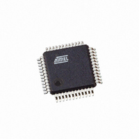
AT91SAM7S32B-AU Atmel, AT91SAM7S32B-AU Datasheet - Page 411

AT91SAM7S32B-AU
Manufacturer Part Number
AT91SAM7S32B-AU
Description
IC MCU ARM7 32KB FLASH 48LQFP
Manufacturer
Atmel
Series
AT91SAMr
Datasheet
1.AT91SAM7S16-MU.pdf
(779 pages)
Specifications of AT91SAM7S32B-AU
Core Processor
ARM7
Core Size
16/32-Bit
Speed
55MHz
Connectivity
I²C, SPI, SSC, UART/USART
Peripherals
Brown-out Detect/Reset, DMA, POR, PWM, WDT
Number Of I /o
21
Program Memory Size
32KB (32K x 8)
Program Memory Type
FLASH
Ram Size
8K x 8
Voltage - Supply (vcc/vdd)
1.65 V ~ 1.95 V
Data Converters
A/D 8x10b
Oscillator Type
Internal
Operating Temperature
-40°C ~ 85°C
Package / Case
48-LQFP
Cpu Family
91S
Device Core
ARM7TDMI
Device Core Size
32b
Frequency (max)
55MHz
Interface Type
SPI/TWI/USART
Total Internal Ram Size
8KB
# I/os (max)
21
Number Of Timers - General Purpose
3
Operating Supply Voltage (typ)
1.8/3.3V
Operating Supply Voltage (max)
1.95/3.6V
Operating Supply Voltage (min)
1.65/3V
On-chip Adc
8-chx10-bit
Instruction Set Architecture
RISC
Operating Temp Range
-40C to 85C
Operating Temperature Classification
Industrial
Mounting
Surface Mount
Pin Count
48
Package Type
LQFP
Package
48LQFP
Family Name
AT91
Maximum Speed
55 MHz
Operating Supply Voltage
1.8|3.3 V
Data Bus Width
32 Bit
Number Of Programmable I/os
21
Number Of Timers
3
For Use With
AT91SAM-ICE - EMULATOR FOR AT91 ARM7/ARM9AT91SAM7S-EK - KIT EVAL FOR ARM AT91SAM7S
Lead Free Status / RoHS Status
Lead free / RoHS Compliant
Eeprom Size
-
Lead Free Status / Rohs Status
Compliant
Available stocks
Company
Part Number
Manufacturer
Quantity
Price
Part Number:
AT91SAM7S32B-AU
Manufacturer:
MICROCHIP/微芯
Quantity:
20 000
- Current page: 411 of 779
- Download datasheet (11Mb)
32.6.1.4
32.6.2
6175K–ATARM–30-Aug-10
Transmitter Operations
Serial Clock Ratio Considerations
Figure 32-7. Receiver Clock Management
The Transmitter and the Receiver can be programmed to operate with the clock signals provided
on either the TK or RK pins. This allows the SSC to support many slave-mode data transfers. In
this case, the maximum clock speed allowed on the RK pin is:
In addition, the maximum clock speed allowed on the TK pin is:
A transmitted frame is triggered by a start event and can be followed by synchronization data
before data transmission.
The start event is configured by setting the Transmit Clock Mode Register (SSC_TCMR).
“Start” on page 413.
The frame synchronization is configured setting the Transmit Frame Mode Register
(SSC_TFMR).
To transmit data, the transmitter uses a shift register clocked by the transmitter clock signal and
the start mode selected in the SSC_TCMR. Data is written by the application to the SSC_THR
register then transferred to the shift register according to the data format selected.
When both the SSC_THR and the transmit shift register are empty, the status flag TXEMPTY is
set in SSC_SR. When the Transmit Holding register is transferred in the Transmit shift register,
the status flag TXRDY is set in SSC_SR and additional data can be loaded in the holding
register.
– Master Clock divided by 2 if Receiver Frame Synchro is input
– Master Clock divided by 3 if Receiver Frame Synchro is output
– Master Clock divided by 6 if Transmit Frame Synchro is input
– Master Clock divided by 2 if Transmit Frame Synchro is output
Transmitter
RK (pin)
Divider
Clock
Clock
See “Frame Sync” on page 415.
MUX
CKS
AT91SAM7S Series Preliminary
CKO
Controller
Tri-state
MUX
CKI
INV
Data Transfer
Controller
Tri-state
CKG
Clock
Output
Receiver
Clock
See
411
Related parts for AT91SAM7S32B-AU
Image
Part Number
Description
Manufacturer
Datasheet
Request
R

Part Number:
Description:
KIT EVAL FOR ARM AT91SAM7S
Manufacturer:
Atmel
Datasheet:

Part Number:
Description:
MCU, MPU & DSP Development Tools KICKSTART KIT ATMEL AT91SAM7S
Manufacturer:
IAR Systems

Part Number:
Description:
DEV KIT FOR AVR/AVR32
Manufacturer:
Atmel
Datasheet:

Part Number:
Description:
INTERVAL AND WIPE/WASH WIPER CONTROL IC WITH DELAY
Manufacturer:
ATMEL Corporation
Datasheet:

Part Number:
Description:
Low-Voltage Voice-Switched IC for Hands-Free Operation
Manufacturer:
ATMEL Corporation
Datasheet:

Part Number:
Description:
MONOLITHIC INTEGRATED FEATUREPHONE CIRCUIT
Manufacturer:
ATMEL Corporation
Datasheet:

Part Number:
Description:
AM-FM Receiver IC U4255BM-M
Manufacturer:
ATMEL Corporation
Datasheet:

Part Number:
Description:
Monolithic Integrated Feature Phone Circuit
Manufacturer:
ATMEL Corporation
Datasheet:

Part Number:
Description:
Multistandard Video-IF and Quasi Parallel Sound Processing
Manufacturer:
ATMEL Corporation
Datasheet:

Part Number:
Description:
High-performance EE PLD
Manufacturer:
ATMEL Corporation
Datasheet:

Part Number:
Description:
8-bit Flash Microcontroller
Manufacturer:
ATMEL Corporation
Datasheet:

Part Number:
Description:
2-Wire Serial EEPROM
Manufacturer:
ATMEL Corporation
Datasheet:


