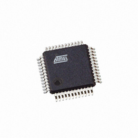
AT91SAM7S32B-AU Atmel, AT91SAM7S32B-AU Datasheet - Page 606

AT91SAM7S32B-AU
Manufacturer Part Number
AT91SAM7S32B-AU
Description
IC MCU ARM7 32KB FLASH 48LQFP
Manufacturer
Atmel
Series
AT91SAMr
Datasheet
1.AT91SAM7S16-MU.pdf
(779 pages)
Specifications of AT91SAM7S32B-AU
Core Processor
ARM7
Core Size
16/32-Bit
Speed
55MHz
Connectivity
I²C, SPI, SSC, UART/USART
Peripherals
Brown-out Detect/Reset, DMA, POR, PWM, WDT
Number Of I /o
21
Program Memory Size
32KB (32K x 8)
Program Memory Type
FLASH
Ram Size
8K x 8
Voltage - Supply (vcc/vdd)
1.65 V ~ 1.95 V
Data Converters
A/D 8x10b
Oscillator Type
Internal
Operating Temperature
-40°C ~ 85°C
Package / Case
48-LQFP
Cpu Family
91S
Device Core
ARM7TDMI
Device Core Size
32b
Frequency (max)
55MHz
Interface Type
SPI/TWI/USART
Total Internal Ram Size
8KB
# I/os (max)
21
Number Of Timers - General Purpose
3
Operating Supply Voltage (typ)
1.8/3.3V
Operating Supply Voltage (max)
1.95/3.6V
Operating Supply Voltage (min)
1.65/3V
On-chip Adc
8-chx10-bit
Instruction Set Architecture
RISC
Operating Temp Range
-40C to 85C
Operating Temperature Classification
Industrial
Mounting
Surface Mount
Pin Count
48
Package Type
LQFP
Package
48LQFP
Family Name
AT91
Maximum Speed
55 MHz
Operating Supply Voltage
1.8|3.3 V
Data Bus Width
32 Bit
Number Of Programmable I/os
21
Number Of Timers
3
For Use With
AT91SAM-ICE - EMULATOR FOR AT91 ARM7/ARM9AT91SAM7S-EK - KIT EVAL FOR ARM AT91SAM7S
Lead Free Status / RoHS Status
Lead free / RoHS Compliant
Eeprom Size
-
Lead Free Status / Rohs Status
Compliant
Available stocks
Company
Part Number
Manufacturer
Quantity
Price
Part Number:
AT91SAM7S32B-AU
Manufacturer:
MICROCHIP/微芯
Quantity:
20 000
- Current page: 606 of 779
- Download datasheet (11Mb)
40.5.2
40.5.2.1
40.5.3
40.5.3.1
40.5.3.2
606
AT91SAM7S Series Preliminary
Embedded Flash Controller (EFC)
Parallel Input/Output Controller (PIO)
EFC: Embedded Flash Access Time 2
PIO: Leakage on PA17 - PA20
PIO: Electrical Characteristics on NRST and PA0-PA16 and PA21-31
To activate sleep mode as soon as possible, it is recommended to write successively, ADC
Mode Register (SLEEP) then ADC Control Register (START bit field); to start an analog-to-digi-
tal conversion, in order put ADC into sleep mode at the end of this conversion.
The Flash memory access time has been reduced as per the table below:
Set the number of Wait States (FWS) according to the frequency requirements described in this
errata.
When PA17, PA18, PA19 or PA20 (the I/O lines multiplexed with the analog inputs) are set as
digital inputs with pull-up disabled, the leakage can be 9 µA in worst case and 90 nA in typical
case per I/O when the I/O is set externally at low level.
Set the I/O to VDDIO by internal or external pull-up.
When NRST or PA0-PA16 or PA21-PA31 are set as digital inputs with pull-up enabled, the volt-
age of the I/O stabilizes at VPull-up.
Vpull-up
This condition causes a leakage through VDDIO. This leakage is 45 µA per pad in worst case at
3.3 V and 25 µA at 1.8V.
I Leakage
Flash Wait
State (FWS)
0
1
2
3
VPull-up Min
VDDIO - 0.65 V
Parameter
I Leakage at 3,3V
I Leakage at 1.8V
Problem Fix/Workaround
Problem Fix/Workaround
Problem Fix/Workaround
Read
Operations
1 cycle
2 cycles
3 cycles
4 cycles
VPull-up Max
VDDIO - 0.45 V
Typ
2.5
1
µA
µA
Maximum Operating
Frequency (MHz)
16
32
48
55
Max
45
25
µA
µA
6175K–ATARM–30-Aug-10
Related parts for AT91SAM7S32B-AU
Image
Part Number
Description
Manufacturer
Datasheet
Request
R

Part Number:
Description:
KIT EVAL FOR ARM AT91SAM7S
Manufacturer:
Atmel
Datasheet:

Part Number:
Description:
MCU, MPU & DSP Development Tools KICKSTART KIT ATMEL AT91SAM7S
Manufacturer:
IAR Systems

Part Number:
Description:
DEV KIT FOR AVR/AVR32
Manufacturer:
Atmel
Datasheet:

Part Number:
Description:
INTERVAL AND WIPE/WASH WIPER CONTROL IC WITH DELAY
Manufacturer:
ATMEL Corporation
Datasheet:

Part Number:
Description:
Low-Voltage Voice-Switched IC for Hands-Free Operation
Manufacturer:
ATMEL Corporation
Datasheet:

Part Number:
Description:
MONOLITHIC INTEGRATED FEATUREPHONE CIRCUIT
Manufacturer:
ATMEL Corporation
Datasheet:

Part Number:
Description:
AM-FM Receiver IC U4255BM-M
Manufacturer:
ATMEL Corporation
Datasheet:

Part Number:
Description:
Monolithic Integrated Feature Phone Circuit
Manufacturer:
ATMEL Corporation
Datasheet:

Part Number:
Description:
Multistandard Video-IF and Quasi Parallel Sound Processing
Manufacturer:
ATMEL Corporation
Datasheet:

Part Number:
Description:
High-performance EE PLD
Manufacturer:
ATMEL Corporation
Datasheet:

Part Number:
Description:
8-bit Flash Microcontroller
Manufacturer:
ATMEL Corporation
Datasheet:

Part Number:
Description:
2-Wire Serial EEPROM
Manufacturer:
ATMEL Corporation
Datasheet:


