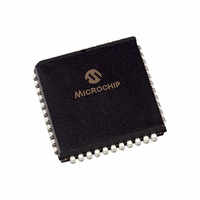
PIC16F877A-I/L Microchip Technology, PIC16F877A-I/L Datasheet - Page 53

PIC16F877A-I/L
Manufacturer Part Number
PIC16F877A-I/L
Description
IC MCU FLASH 8KX14 EE 44PLCC
Manufacturer
Microchip Technology
Series
PIC® 16Fr
Datasheets
1.PIC16F616T-ISL.pdf
(8 pages)
2.PIC16F688T-ISL.pdf
(688 pages)
3.PIC16C770-ISO.pdf
(8 pages)
4.PIC16F873A-ISO.pdf
(234 pages)
5.PIC16F873A-ISO.pdf
(6 pages)
6.PIC16F873A-ISO.pdf
(4 pages)
7.PIC16F873A-ISO.pdf
(6 pages)
8.PIC16F873A-ISO.pdf
(4 pages)
9.PIC16F873A-ISO.pdf
(22 pages)
Specifications of PIC16F877A-I/L
Program Memory Type
FLASH
Program Memory Size
14KB (8K x 14)
Package / Case
44-PLCC
Core Processor
PIC
Core Size
8-Bit
Speed
20MHz
Connectivity
I²C, SPI, UART/USART
Peripherals
Brown-out Detect/Reset, POR, PWM, WDT
Number Of I /o
33
Eeprom Size
256 x 8
Ram Size
368 x 8
Voltage - Supply (vcc/vdd)
4 V ~ 5.5 V
Data Converters
A/D 8x10b
Oscillator Type
External
Operating Temperature
-40°C ~ 85°C
Processor Series
PIC16F
Core
PIC
Data Bus Width
8 bit
Data Ram Size
368 B
Interface Type
I2C/SPI/USART
Maximum Clock Frequency
20 MHz
Number Of Programmable I/os
33
Number Of Timers
3
Operating Supply Voltage
2 V to 5.5 V
Maximum Operating Temperature
+ 85 C
Mounting Style
SMD/SMT
3rd Party Development Tools
52715-96, 52716-328, 52717-734
Development Tools By Supplier
PG164130, DV164035, DV244005, DV164005, PG164120, ICE2000, DM163022, DV164120
Minimum Operating Temperature
- 40 C
On-chip Adc
8-ch x 10-bit
Package
44PLCC
Device Core
PIC
Family Name
PIC16
Maximum Speed
20 MHz
Lead Free Status / RoHS Status
Lead free / RoHS Compliant
For Use With
AC164309 - MODULE SKT FOR PM3 44PLCC444-1001 - DEMO BOARD FOR PICMICRO MCUDVA16XL441 - ADAPTER DEVICE ICE 44PLCC309-1040 - ADAPTER 44-PLCC ZIF TO 40-DIP309-1039 - ADAPTER 44-PLCC TO 40-DIPDV007003 - PROGRAMMER UNIVERSAL PROMATE II
Lead Free Status / Rohs Status
Lead free / RoHS Compliant
Other names
PIC16F877AI/L
Available stocks
Company
Part Number
Manufacturer
Quantity
Price
Company:
Part Number:
PIC16F877A-I/L
Manufacturer:
NEC
Quantity:
1 600
Company:
Part Number:
PIC16F877A-I/L
Manufacturer:
Microchip Technology
Quantity:
10 000
Company:
Part Number:
PIC16F877A-I/LG
Manufacturer:
Microchip Technology
Quantity:
10 000
4.6
The Parallel Slave Port (PSP) is not implemented on
the PIC16F873A or PIC16F876A.
PORTD operates as an 8-bit wide Parallel Slave Port,
or microprocessor port, when control bit PSPMODE
(TRISE<4>) is set. In Slave mode, it is asynchronously
readable and writable by the external world through RD
control input pin, RE0/RD/AN5, and WR control input
pin, RE1/WR/AN6.
The
microprocessor data bus. The external microprocessor
can read or write the PORTD latch as an 8-bit latch.
Setting bit PSPMODE enables port pin RE0/RD/AN5 to
be the RD input, RE1/WR/AN6 to be the WR input and
RE2/CS/AN7 to be the CS (Chip Select) input. For this
functionality, the corresponding data direction bits of
the TRISE register (TRISE<2:0>) must be configured
as inputs (set). The A/D port configuration bits,
PCFG3:PCFG0 (ADCON1<3:0>), must be set to
configure pins RE2:RE0 as digital I/O.
There are actually two 8-bit latches: one for data output
and one for data input. The user writes 8-bit data to the
PORTD data latch and reads data from the port pin
latch (note that they have the same address). In this
mode, the TRISD register is ignored since the external
device is controlling the direction of data flow.
A write to the PSP occurs when both the CS and WR
lines are first detected low. When either the CS or WR
lines become high (level triggered), the Input Buffer Full
(IBF) status flag bit (TRISE<7>) is set on the Q4 clock
cycle, following the next Q2 cycle, to signal the write is
complete (Figure 4-11). The interrupt flag bit, PSPIF
(PIR1<7>), is also set on the same Q4 clock cycle. IBF
can only be cleared by reading the PORTD input latch.
The Input Buffer Overflow (IBOV) status flag bit
(TRISE<5>) is set if a second write to the PSP is
attempted when the previous byte has not been read
out of the buffer.
A read from the PSP occurs when both the CS and RD
lines are first detected low. The Output Buffer Full
(OBF)
immediately (Figure 4-12), indicating that the PORTD
latch is waiting to be read by the external bus. When
either the CS or RD pin becomes high (level triggered),
the interrupt flag bit PSPIF is set on the Q4 clock cycle,
following the next Q2 cycle, indicating that the read is
complete. OBF remains low until data is written to
PORTD by the user firmware.
2003 Microchip Technology Inc.
PSP
status
Parallel Slave Port
can
flag
directly
bit
(TRISE<6>)
interface
to
is
an
cleared
8-bit
When not in PSP mode, the IBF and OBF bits are held
clear. However, if flag bit IBOV was previously set, it
must be cleared in firmware.
An interrupt is generated and latched into flag bit
PSPIF when a read or write operation is completed.
PSPIF must be cleared by the user in firmware and the
interrupt can be disabled by clearing the interrupt
enable bit PSPIE (PIE1<7>).
FIGURE 4-10:
Note 1: I/O pins have protection diodes to V
One bit of PORTD
Data Bus
Set Interrupt Flag
PSPIF (PIR1<7>)
RD Port
WR
Port
Q
D
CK
EN
EN
PIC16F87XA
Q
PORTD AND PORTE
BLOCK DIAGRAM
(PARALLEL SLAVE PORT)
D
Chip Select
Read
Write
DS39582B-page 51
TTL
DD
TTL
TTL
TTL
and V
SS
RDx pin
.
RD
CS
WR


